Boosting circuit

Active Publication Date: 2010-07-29
ABLIC INC
View PDF3 Cites 0 Cited by
  • Summary
  • Abstract
  • Description
  • Claims
  • Application Information

AI Technical Summary

Benefits of technology

[0018]According to the present invention, the reset transistor for resetting the gate of the charge transfer transistor after the boosting operation has been finished is configured to reset the gate of the charge transfer transistor when turned ON through the application of the power supply voltage to the gate of the reset transistor. Therefore, another boosted voltage is not required for the reset, and hence an additional boosting circuit required for the another boosted voltage is unnecessary as well.

Problems solved by technology

Therefore, an additional boosting circuit is required for the reset, which arises a problem that a circuit scale of the boosting circuit is increased correspondingly to the additional boosting circuit.

Method used


Image

  • Boosting circuit
  • Boosting circuit
  • Boosting circuit

Examples


Embodiment Construction

[0027]Now, referring to the accompanying drawings, an embodiment of the present invention is described below.

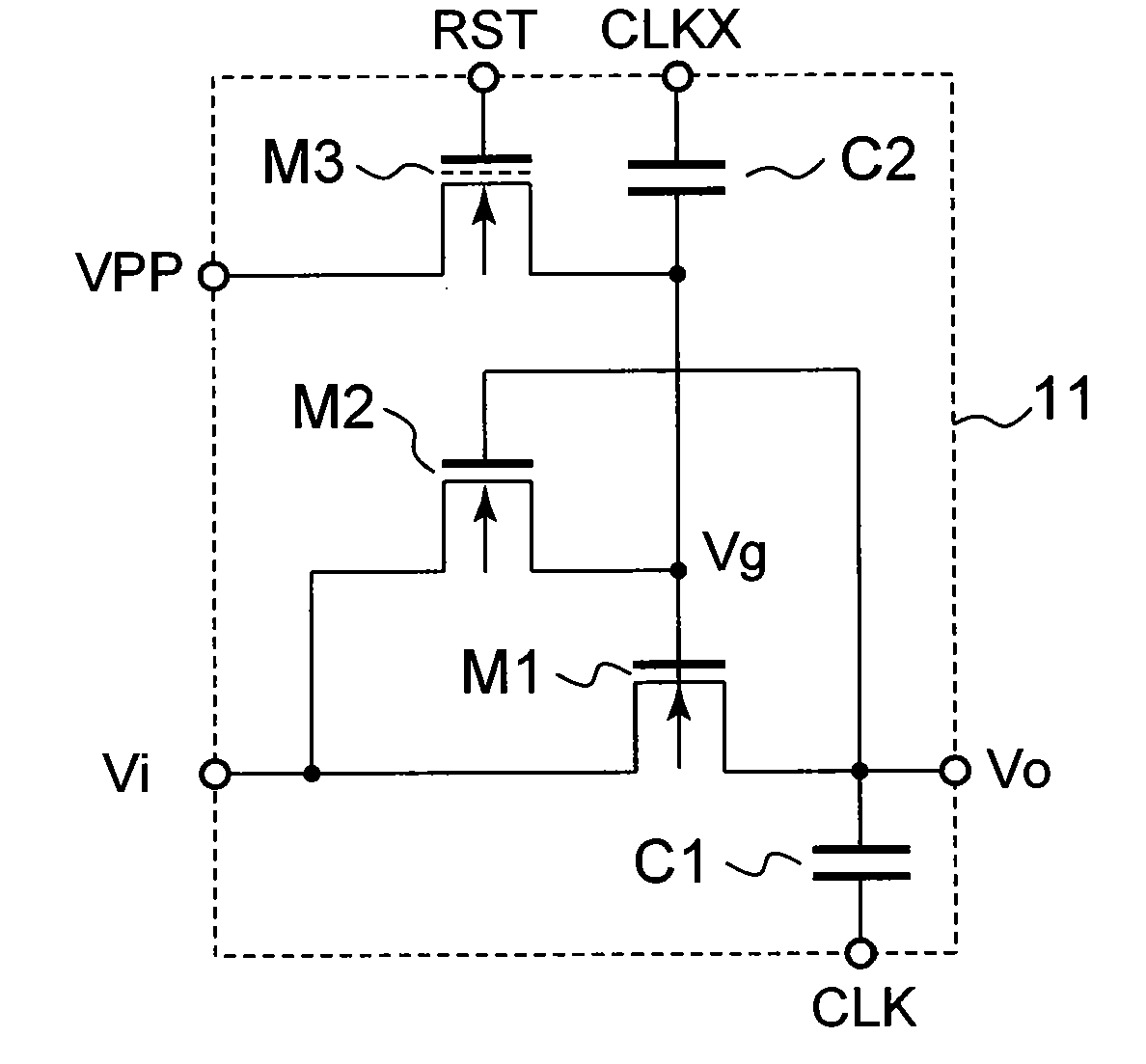
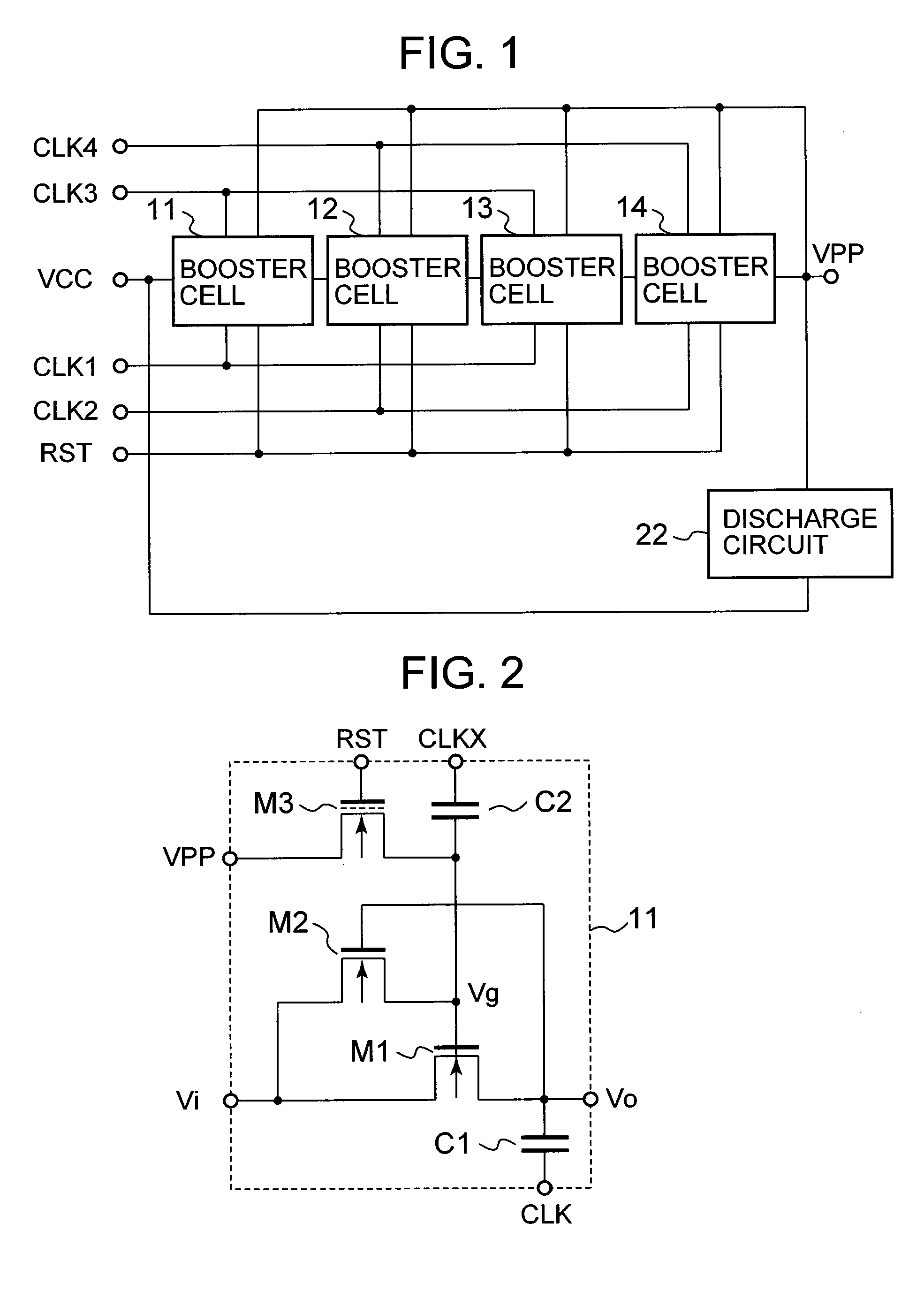
[0028]First, a configuration of a boosting circuit according to the embodiment of the present invention is described. FIG. 1 is a diagram illustrating the boosting circuit.

[0029]The boosting circuit includes a power supply terminal VCC, a boost terminal VPP, clock terminals CLK1 to CLK4, and a reset terminal RST. The boosting circuit further includes booster cells 11 to 14 and a discharge circuit 22.

[0030]The clock terminal CLK1 is connected to respective internal clock terminals CLK of the booster cell 11 and the booster cell 13. The clock terminal CLK2 is connected to respective internal clock terminals CLK of the booster cell 12 and the booster cell 14.

[0031]The clock terminal CLK3 is connected to respective internal clock terminals CLKX of the booster cell 11 and the booster cell 13. The clock terminal CLK4 is connected to respective internal clock terminals CLKX of the b...


PUM


Abstract

Provided is a boosting circuit having a small circuit scale. When a node (Vg) is reset by a reset transistor (M3) after a boosting operation has been finished, the reset transistor (M3) is controlled based on a power supply voltage to reset the node (Vg). Therefore, another boosted voltage is not required for the reset, and hence an additional boosting circuit required for the another boosted voltage is unnecessary as well. As a result, the circuit scale of the boosting circuit is reduced correspondingly to the additional boosting circuit.

Description

RELATED APPLICATIONS[0001]This application claims priority under 35 U.S.C. §119 to Japanese Patent Application No. 2009-018243 filed on Jan. 29, 2009, the entire content of which is hereby incorporated by reference.BACKGROUND OF THE INVENTION[0002]1. Field of the Invention[0003]The present invention relates to a boosting circuit, and more specifically, to a boosting circuit for outputting a boosted voltage higher than a power supply voltage from a boost terminal.[0004]2. Description of the Related Art[0005]At present, in a semiconductor device, there may be employed a boosting circuit for outputting a boosted voltage higher than a power supply voltage from a boost terminal. For example, in a non-volatile semiconductor device, the boosting circuit is installed because the boosted voltage is used at the time of writing / erasing into / from a memory cell transistor.[0006]A known example of such boosting circuit is a threshold offset type boosting circuit, which is driven in response to fo...

Claims


Application Information

Patent Timeline
IPC IPC(8): G05F1/10
CPCH02M3/07
Inventor MITANI, MAKOTOUTSUNOMIYA, FUMIYASU
Owner ABLIC INC
Why Eureka
Try Eureka