3d-integrated optical sensor and method of producing a 3d-integrated optical sensor
- Summary
- Abstract
- Description
- Claims
- Application Information
AI Technical Summary
Benefits of technology
Problems solved by technology
Method used
Image
Examples
Embodiment Construction
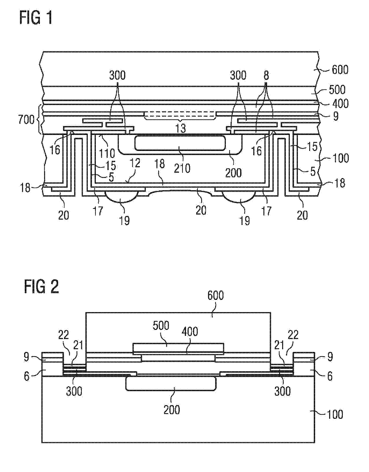
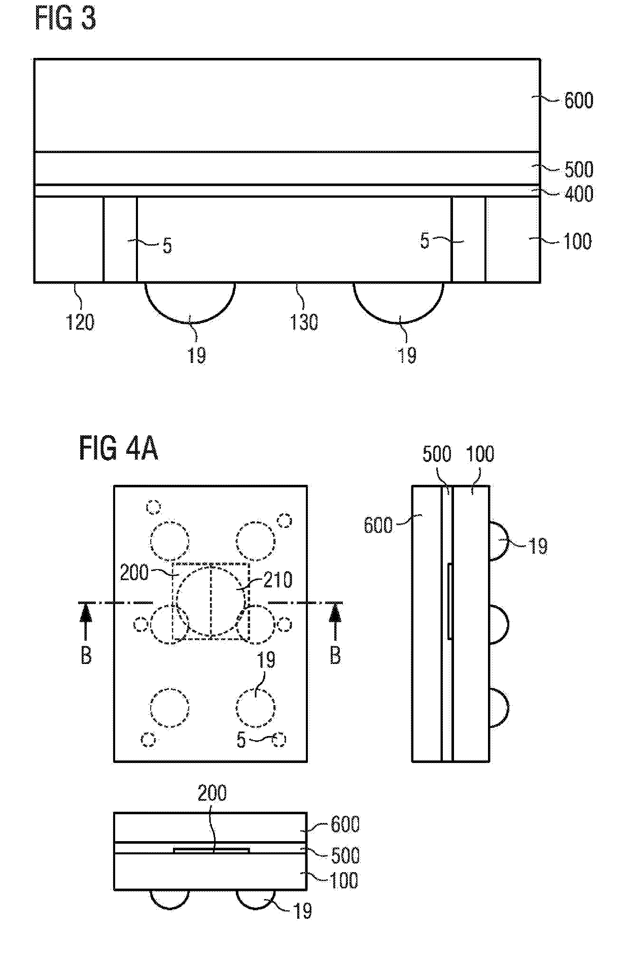
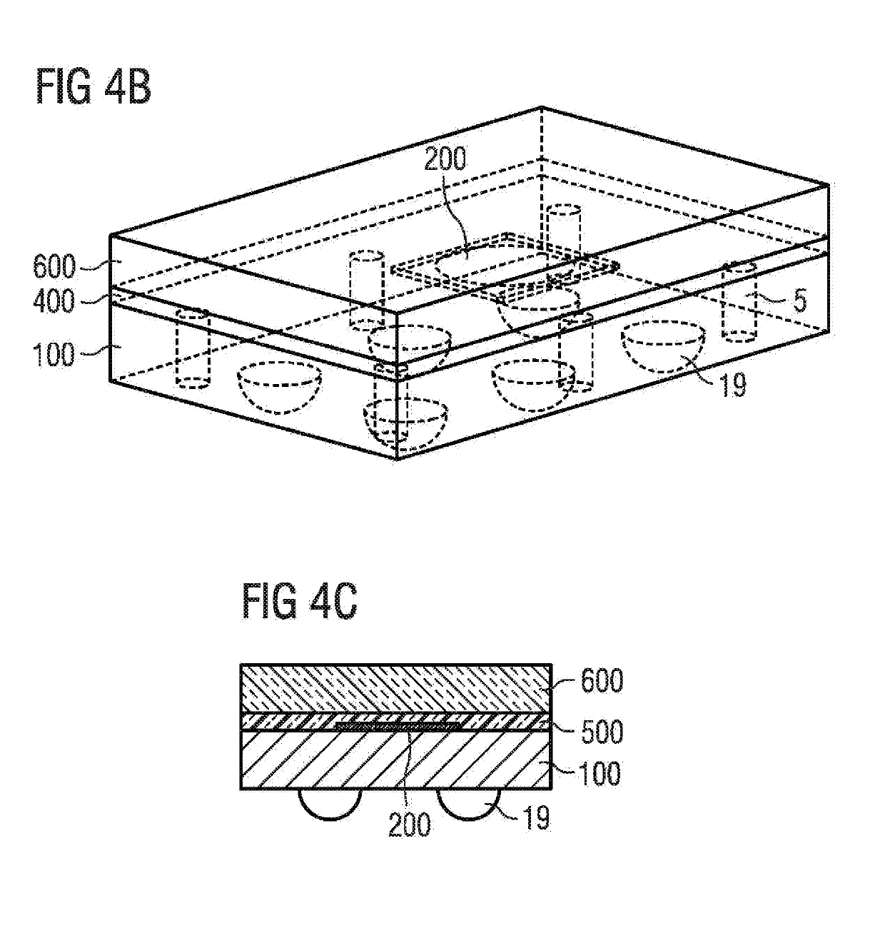
[0044]FIG. 1 shows an exemplary embodiment of an optical sensor. The 3D integrated optical sensor comprises a semiconductor substrate 100, an integrated circuit 200, a wiring 300, a filter layer 400, a transparent spacer layer 500, and a diffuser 600. In this particular embodiment the optical sensor also comprises a dielectric layer 700 and several through silicon vias.
[0045]The semiconductor substrate 100 has a main surface 110. The integrated circuit 200 is arranged in the semiconductor substrate 100 near the main surface 110. The integrated circuit 200 has a light sensitive area 210. Typically, the semiconductor substrate 100 constitutes a silicon wafer, or part of a silicon wafer. In this particular embodiment the integrated circuit comprises one or more photodiodes, e.g. photodiodes sensitive in the visual or near infrared range of the electromagnetic spectrum. The photodiodes may be integrated in a CMOS process technology. A single or a plurality of integrated optical sensors ...
PUM
 Abstract
Description
Claims
Application Information
 - R&D
- Intellectual Property
- Life Sciences
- Materials
- Tech Scout
- Unparalleled Data Quality
- Higher Quality Content
- 60% Fewer Hallucinations
Browse by: Latest US Patents, China's latest patents, Technical Efficacy Thesaurus, Application Domain, Technology Topic, Popular Technical Reports.
© 2025 PatSnap. All rights reserved.Legal|Privacy policy|Modern Slavery Act Transparency Statement|Sitemap|About US| Contact US: help@patsnap.com


