Distortion compensation circuit
a compensation circuit and resistor technology, applied in the direction of amplifiers, amplifier types, electrical devices, etc., can solve the problems of reducing the distortion characteristics, and reducing so as to achieve the effect of lessening the effect of reducing the distortion by the resistor
- Summary
- Abstract
- Description
- Claims
- Application Information
AI Technical Summary
Benefits of technology
Problems solved by technology
Method used
Image
Examples
first embodiment
[0027][1-1. Configuration]
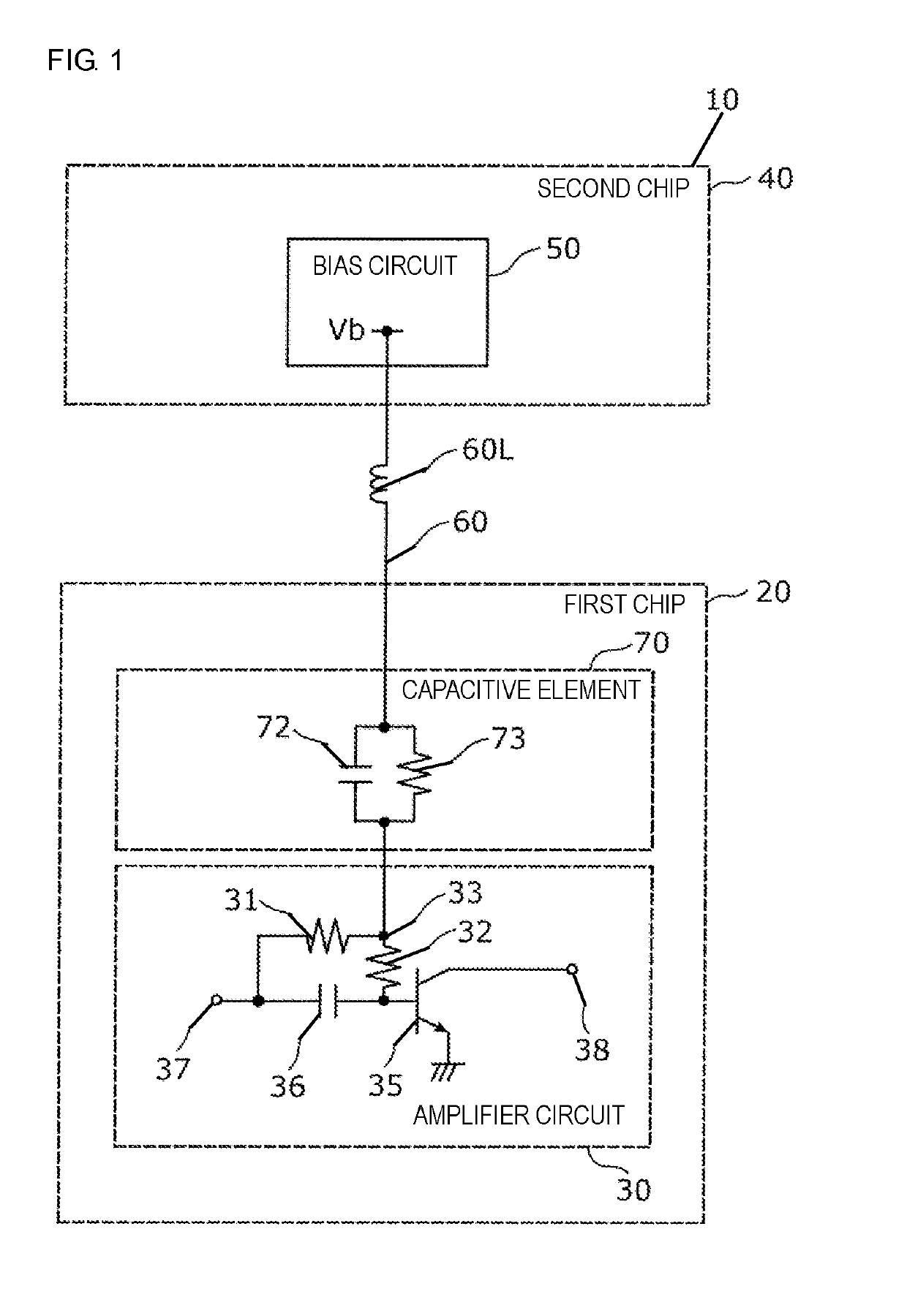
[0028]The configuration of a distortion compensation circuit 10 according to a first embodiment will be described below with reference to FIG. 1. FIG. 1 is a schematic circuit diagram illustrating the configuration of the distortion compensation circuit 10 according to the first embodiment. As shown in FIG. 1, the distortion compensation circuit 10 includes an amplifier circuit 30, a bias circuit 50, a wiring 60, and a capacitive element 70. In the first embodiment, the distortion compensation circuit 10 includes a first chip 20 and a second chip 40. The first chip 20 includes the amplifier circuit 30. The second chip 40, which is different from the first chip 20, includes the bias circuit 50.
[0029]The amplifier circuit 30 amplifies an input signal. In the first embodiment, the amplifier circuit 30 is a power amplifier which amplifies a 5-GHz radio-frequency (RF) signal, for example. The amplifier circuit 30 includes an input terminal 37, an output terminal...
second embodiment
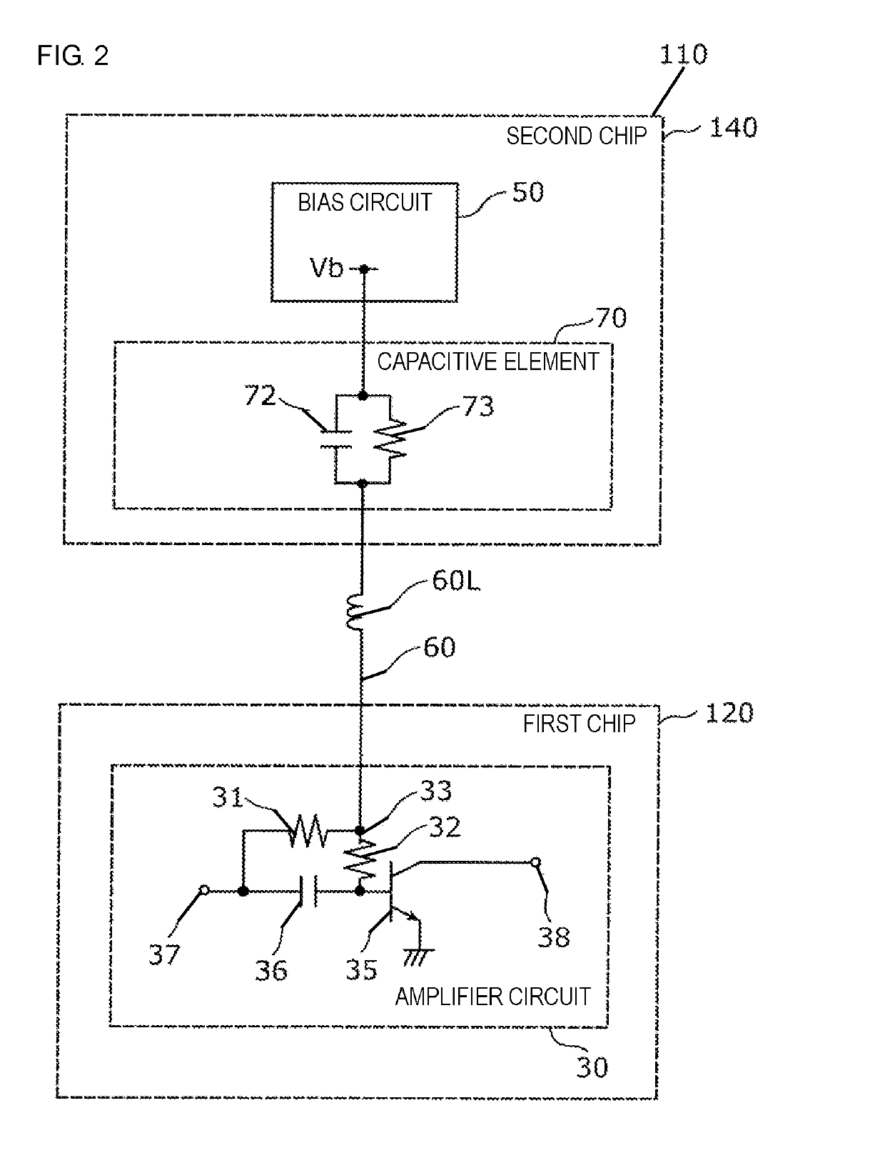
[0046]A distortion compensation circuit 110 according to a second embodiment will be described below. The configuration of the distortion compensation circuit 110 is similar to that of the distortion compensation circuit 10 of the first embodiment, except for the position of the capacitive element 70. The distortion compensation circuit 110 of the second embodiment will now be discussed below with reference to FIG. 2 mainly by referring to points different from the distortion compensation circuit 10 of the first embodiment.
[0047]FIG. 2 is a schematic circuit diagram illustrating the configuration of the distortion compensation circuit 110 according to the second embodiment. As shown in FIG. 2, the distortion compensation circuit 110 includes an amplifier circuit 30, a bias circuit 50, a wiring 60, and a capacitive element 70. In the second embodiment, the amplifier circuit 30 is included in a first chip 120, while the bias circuit 50 and the capacitive element 70 are included in a s...
third embodiment
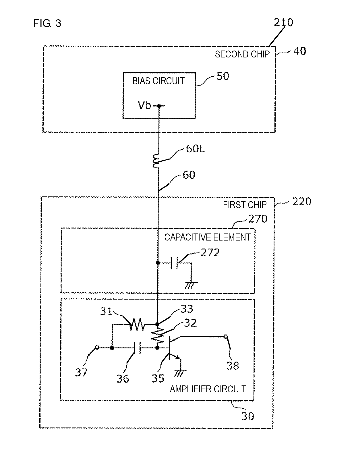
[0050]A distortion compensation circuit 210 according to a third embodiment will be described below. The configuration of the distortion compensation circuit 210 is similar to that of the distortion compensation circuit 10 of the first embodiment, except for the configuration of a capacitive element 270. The distortion compensation circuit 210 of the third embodiment will now be discussed below with reference to FIG. 3 mainly by referring to points different from the distortion compensation circuit 10 of the first embodiment.
[0051]FIG. 3 is a schematic circuit diagram illustrating the configuration of the distortion compensation circuit 210 according to the third embodiment. As shown in FIG. 3, the distortion compensation circuit 210 includes an amplifier circuit 30, a bias circuit 50, a wiring 60, and a capacitive element 270. In the third embodiment, the amplifier circuit 30 and the capacitive element 270 are included in a first chip 220, while the bias circuit 50 is included in a...
PUM
 Abstract
Description
Claims
Application Information
 - R&D
- Intellectual Property
- Life Sciences
- Materials
- Tech Scout
- Unparalleled Data Quality
- Higher Quality Content
- 60% Fewer Hallucinations
Browse by: Latest US Patents, China's latest patents, Technical Efficacy Thesaurus, Application Domain, Technology Topic, Popular Technical Reports.
© 2025 PatSnap. All rights reserved.Legal|Privacy policy|Modern Slavery Act Transparency Statement|Sitemap|About US| Contact US: help@patsnap.com


