Back-channel-etched TFT substrate and manufacturing method thereof

Inactive Publication Date: 2019-05-23
SHENZHEN CHINA STAR OPTOELECTRONICS SEMICON DISPLAY TECH CO LTD
View PDF6 Cites 1 Cited by
  • Summary
  • Abstract
  • Description
  • Claims
  • Application Information

AI Technical Summary

Benefits of technology

The present invention provides a manufacturing method of the back-channel-etched (BCE) TFT substrate that ensures the active layer not damaged in the source / drain etching process, keeps the active layer stable, and results in stable electric properties of the manufactured BCE TFT substrate while keeping production cost low. The invention also provides a BCE TFT substrate with stable electric properties and low production cost. The method uses the C-axis crystallized IGZO thin film as the active layer, which has high corrosion resistance and resistance to the erosion of the copper etchant, resulting in stable performance of the active layer. The substrate is prepared under a high oxygen atmosphere to reduce the crystallization annealing temperature of the amorphous IGZO thin film to 600°C or below, saving on high-temperature annealing furnace and reducing production cost.

Problems solved by technology

However, with the development of the LCD device towards large size (75 inches or more) and high resolution (8K4K), and the use of copper (Cu) in the source and drain, the only about 1 cm2 / (Vs) mobility of the conventional a-Si has been unable to meet the requirements, while the metal oxide material, such as, indium gallium zinc oxide (IGZO) with the more than 15 cm2 / (Vs) mobility, and the corresponding TFT fabrication compatibility with existing production line of a-Si semiconductors, has rapidly become the focus of research and development in recent years.
However, the manufacturing process of IGZO TFT with ESL structure is complicated and requires six photolithography processes, which is disabling for cost reduction.
However, the known copper etching solution inevitably affects the active layer of the IGZO and causes a certain amount of etching to change the surface characteristics of the active layer of the IGZO so that the stability of the TFT substrate is deteriorated.

Method used


Image

  • Back-channel-etched TFT substrate and manufacturing method thereof
  • Back-channel-etched TFT substrate and manufacturing method thereof
  • Back-channel-etched TFT substrate and manufacturing method thereof

Examples


Embodiment Construction

[0042]To further explain the technique means and effect of the present invention, the following uses preferred embodiments and drawings for detailed description.

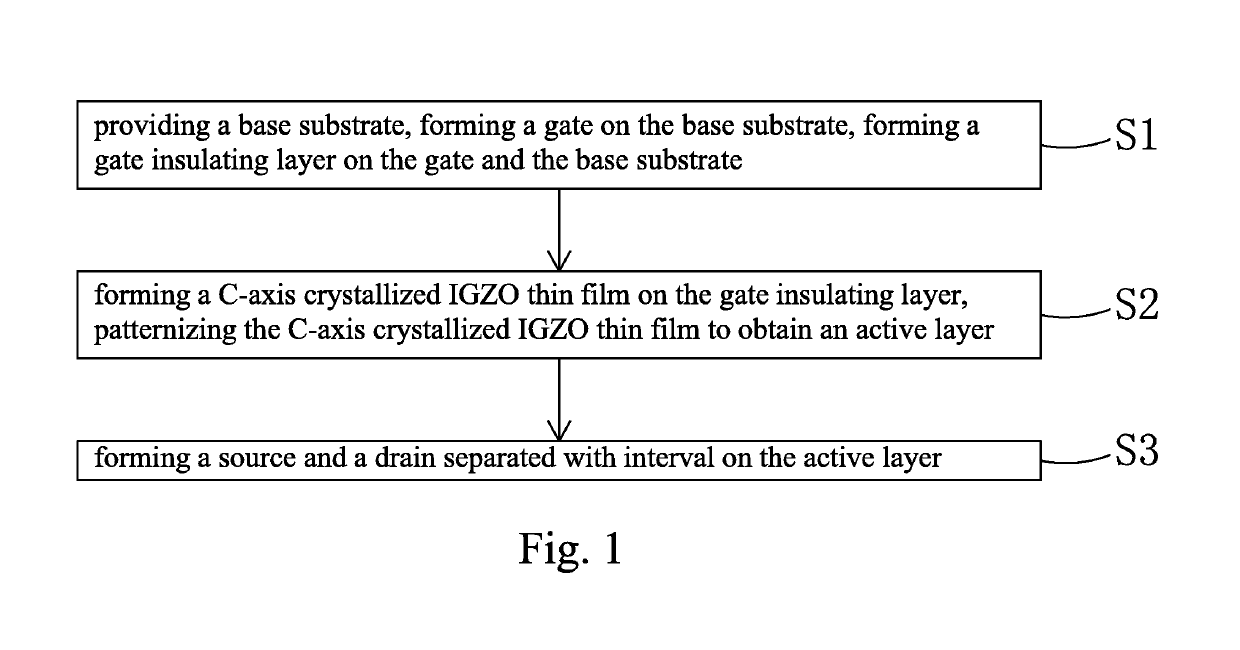
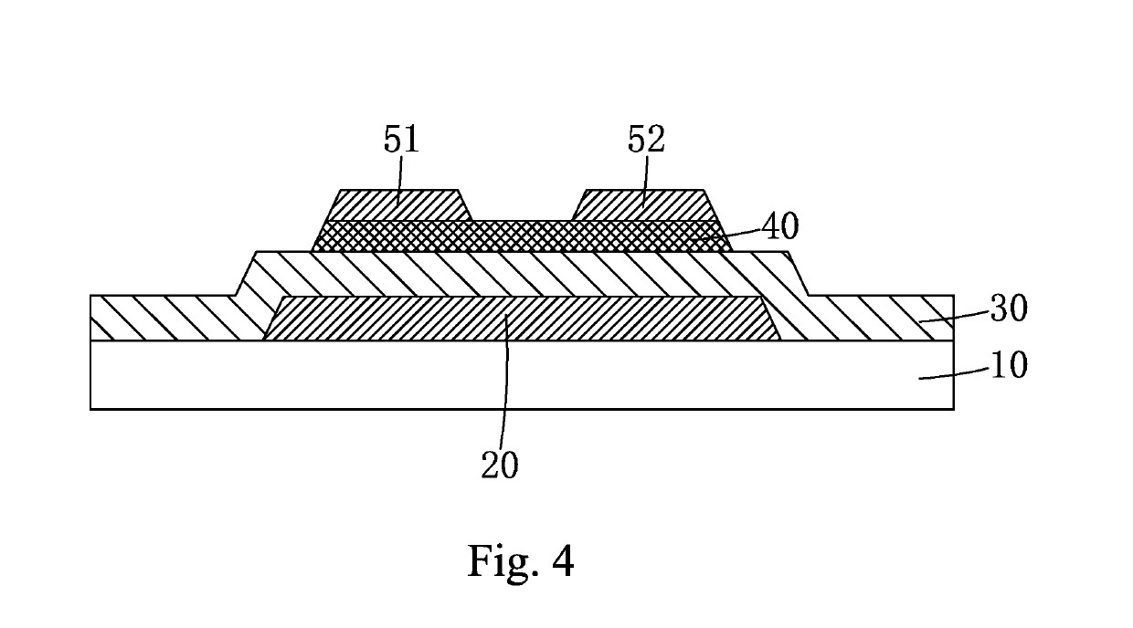
[0043]Referring to FIG. 1, the present invention provides a manufacturing method of back-channel-etched TFT substrate, comprising:

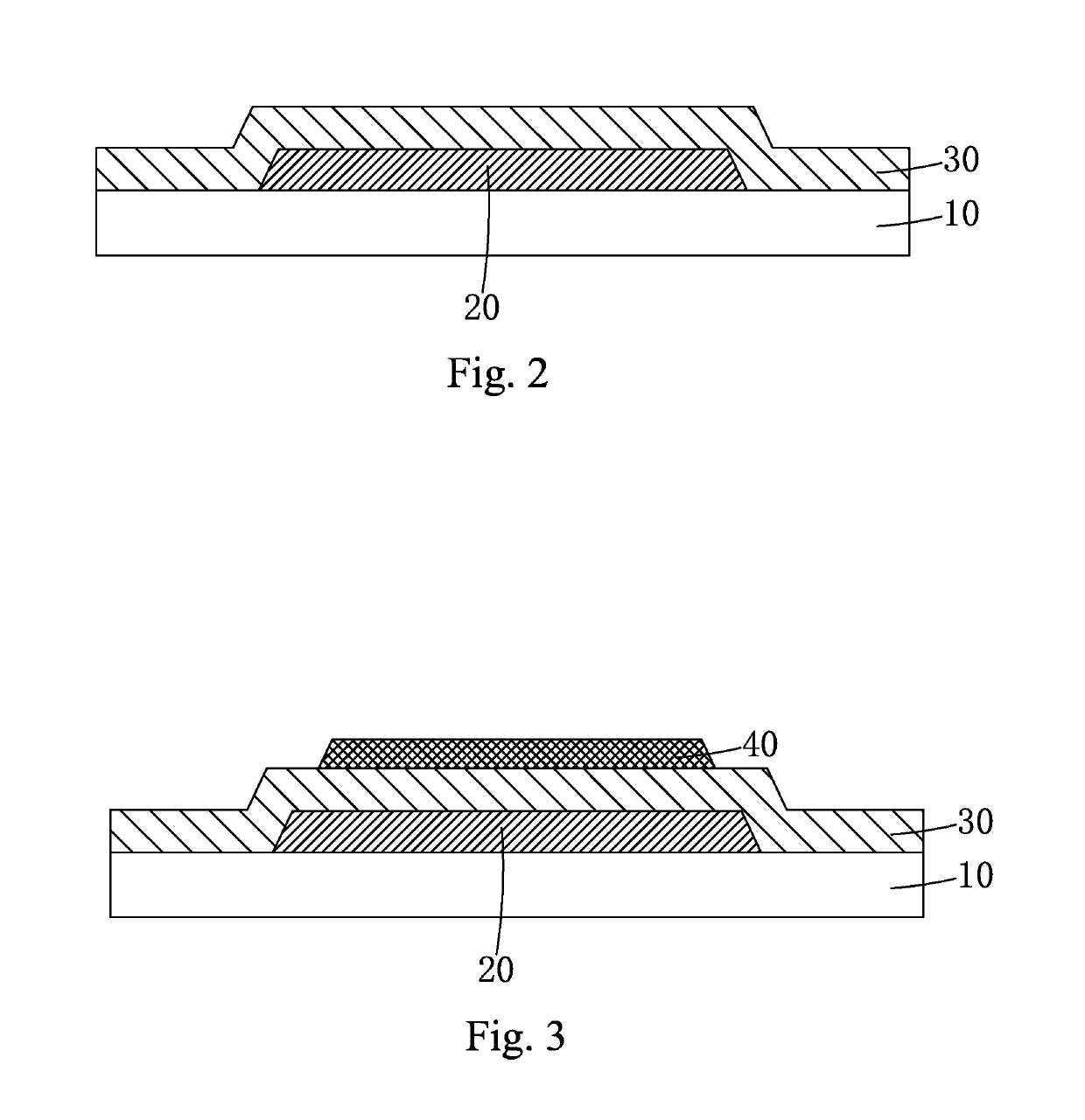
[0044]Step S1: as shown in FIG. 2, providing a base substrate 10, forming a gate 20 on the base substrate 10, forming a gate insulating layer 30 on the gate 20 and the base substrate 10.

[0045]Specifically, the base substrate 10 is a glass substrate.

[0046]Specifically, the materials for the gate 20 comprise one or more of the following: Mo, Al, Cu, Ti, and Cr.

[0047]Specifically, the step of forming the gate 20 on the base substrate 10 comprises: depositing a first metal thin film on the base substrate 10, using a photo-etching process to patternize the first metal thin film to obtain the gate 20.

[0048]Specifically, the gate insulating layer 30 is an SiOx, layer, a SiNx, layer, or a complex layer fo...


PUM


Abstract

The invention provides a BCE TFT substrate and manufacturing method thereof. The manufacturing method of BCE TFT substrate of the invention uses C-axis crystallized IGZO thin film to fabricate the active layer. Because the C-axis crystallized IGZO has extremely high corrosion resistance and is resistant to the erosion of the copper etchant, the active layer is not damaged in the source / drain etching process, and the performance of the active layer is stable. The manufactured BCE TFT substrate has stable electric performance. The amorphous IGZO thin film for fabricating the C-axis crystallized IGZO thin film is prepared under high oxygen atmosphere, so that the crystallization annealing temperature of the amorphous IGZO thin film is reduced to 600° C. or below. A high-temperature annealing furnace is saved and the production cost reduced. The BCE TFT substrate of the invention manufactured by the above method has stable electric performance and low production cost.

Description

BACKGROUND OF THE INVENTION1. Field of the Invention[0001]The present invention relates to the field of display techniques, and in particular to a back-channel-etched thin film transistor (TFT) substrate and manufacturing method thereof.2. The Related Arts[0002]The liquid crystal display (LCD) provides advantages of thinness, low power-consumption and no radiation, and is widely used in, such as, LCD televisions, mobile phones, personal digital assistants (PDAs), digital cameras, computer screens, laptop screens, and so on.[0003]Most of the LCDs on the current market are of backlight type, which comprises an LCD panel and a backlight module. The operation theory behind LCD is to inject the liquid crystal (LC) molecules between a thin film transistor (TFT) array substrate and a color filter (CF) substrate, and applies a driving voltage between the two substrates to control the rotation direction of the LC molecules to refract the light from the backlight module to generate the image ...

Claims


Application Information

Patent Timeline
IPC IPC(8): H01L29/66H01L27/12H01L21/3213H01L29/45H01L29/786
CPCH01L29/66969H01L27/1262H01L21/3213H01L29/45H01L29/7869H01L21/02422H01L21/02488H01L21/02554H01L21/02565H01L21/02609H01L21/02631H01L21/02667H01L29/045
Inventor JIANG, CHUNSHENG
Owner SHENZHEN CHINA STAR OPTOELECTRONICS SEMICON DISPLAY TECH CO LTD
Why Eureka
Try Eureka