Plasma deposition of carbon hardmask

a technology of carbon hardmask and plasma, which is applied in the direction of chemical vapor deposition coating, vacuum evaporation coating, coating, etc., can solve the problems of insufficient thin resist layer to mask the underlying material layer, lack of desired etch selectivity of current hardmask materials, and complex devices of integrated circuits

Active Publication Date: 2019-02-21
APPLIED MATERIALS INC
View PDF7 Cites 6 Cited by
  • Summary
  • Abstract
  • Description
  • Claims
  • Application Information

AI Technical Summary

Benefits of technology

The present disclosure provides techniques for placing high-density films on substrates for patterning applications. Two methods are presented: one involves using an electron beam plasma to create a transparent carbon layer on a substrate, and another involves creating a hardmask layer from a transparent carbon layer. Additionally, a chemical vapor deposition process is described for placing a carbon layer and a physical vapor deposition process is described for creating a carbon hardmask layer. These techniques are useful in semiconductor applications.

Problems solved by technology

Integrated circuits have evolved into complex devices that can include millions of transistors, capacitors and resistors on a single chip.
Such thin resist layers can be insufficient to mask underlying material layers during the pattern transfer step due to attack by the chemical etchant.
As critical dimensions (CD) decrease, current hardmask materials lack the desired etch selectivity relative to underlying materials (e.g., oxides and nitrides) and are often difficult to deposit.

Method used


Image

  • Plasma deposition of carbon hardmask
  • Plasma deposition of carbon hardmask
  • Plasma deposition of carbon hardmask

Examples


Embodiment Construction

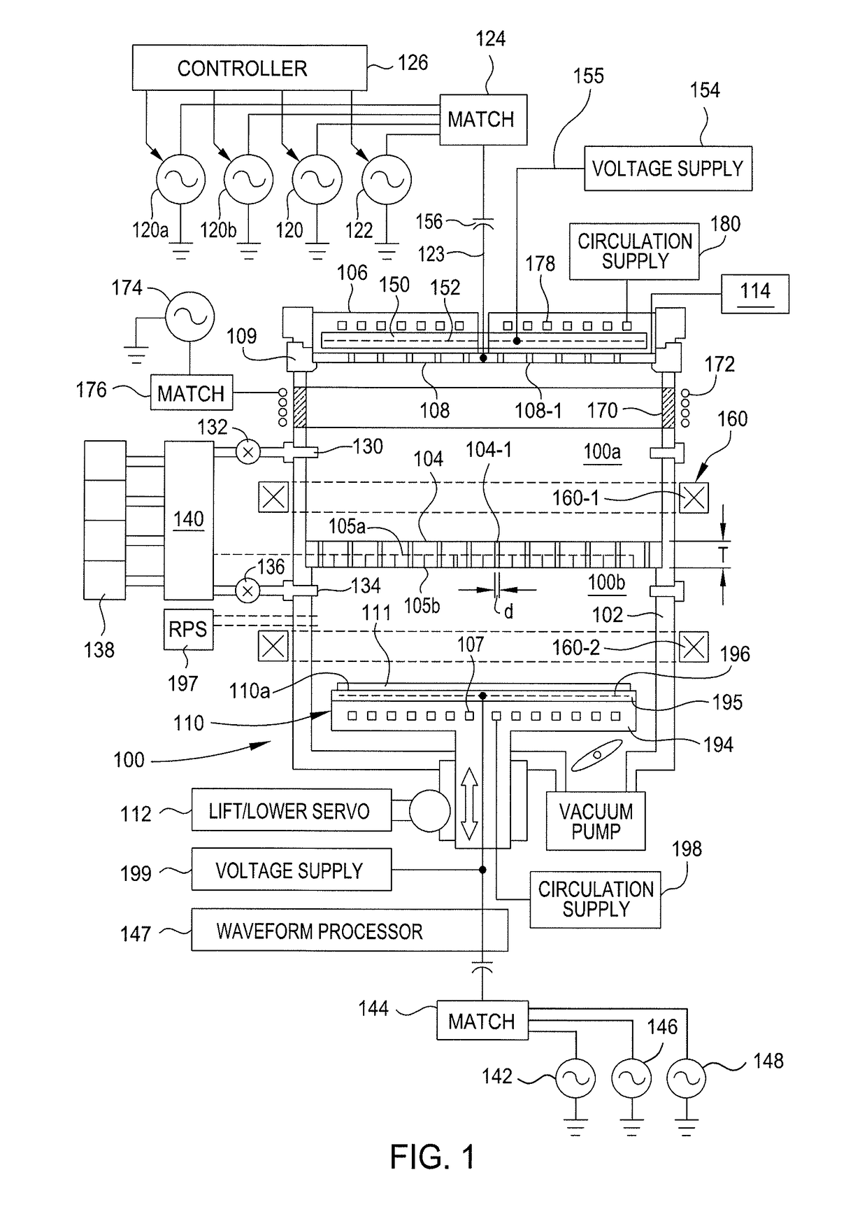
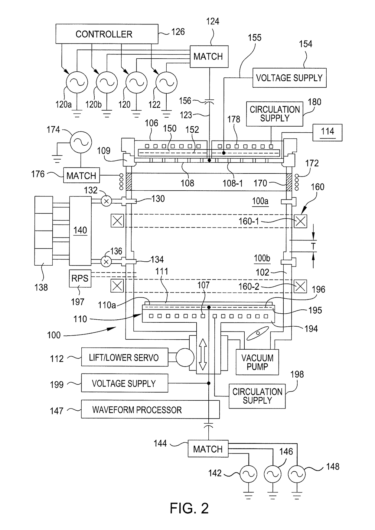
[0019]The following disclosure describes method for forming carbon-containing hardmask layers. Certain details are set forth in the following description and in FIGS. 1-6C to provide a thorough understanding of various implementations of the disclosure. Other details describing well-known structures and systems often associated with chemical vapor deposition and physical vapor deposition are not set forth in the following disclosure to avoid unnecessarily obscuring the description of the various implementations.

[0020]Many of the details, dimensions, angles and other features shown in the Figures are merely illustrative of particular implementations. Accordingly, other implementations can have other details, components, dimensions, angles and features without departing from the spirit or scope of the present disclosure. In addition, further implementations of the disclosure can be practiced without several of the details described below.

[0021]Ashable hardmask films are used in semico...


PUM

PropertyMeasurementUnit
Pressureaaaaaaaaaa
Densityaaaaaaaaaa
Frequencyaaaaaaaaaa

Abstract

A method of forming a transparent carbon layer on a substrate is provided. The method comprises generating an electron beam plasma above a surface of a substrate positioned over a first electrode and disposed in a processing chamber having a second electrode positioned above the first electrode. The method further comprises flowing a hydrocarbon-containing gas mixture into the processing chamber, wherein the second electrode has a surface containing a secondary electrode emission material selected from a silicon-containing material and a carbon-containing material. The method further comprises applying a first RF power to at least one of the first electrode and the second electrode and forming a transparent carbon layer on the surface of the substrate.

Description

CROSS-REFERENCE TO RELATED APPLICATIONS[0001]This application claims benefit of U.S. Provisional Patent Application Ser. No. 62 / 546,266, filed Aug. 16, 2017, which is incorporated herein by reference in its entirety.BACKGROUNDField[0002]Implementations of the present disclosure generally relate to the fabrication of integrated circuits. More particularly, the implementations described herein provide techniques for deposition of high-density films for patterning applications.Description of the Related Art[0003]Integrated circuits have evolved into complex devices that can include millions of transistors, capacitors and resistors on a single chip. The evolution of chip designs continually involves faster circuitry and greater circuit density. The demands for faster circuits with greater circuit densities impose corresponding demands on the materials used to fabricate such integrated circuits. In particular, as the dimensions of integrated circuit components are reduced to the sub-micr...

Claims


Application Information

Patent Timeline
IPC IPC(8): H01L21/02H01J37/32H01L21/3213H01L21/311H01L21/033C23C16/26C23C16/505C23C16/52
CPCC23C16/505C23C16/52H01J2237/3321H01L21/31144H01L21/02274H01J37/32568C23C16/26H01J37/32724H01J37/3266H01L21/32139H01J2237/3341H01L21/0337H01J37/32458C23C14/0605C23C14/345C23C16/4405H01L21/02115H01L21/02266H01L21/0332
Inventor YANG, YANGVENKATASUBRAMANIAN, ESWARANANDRAMASWAMY, KARTIKCOLLINS, KENNETH S.LANE, STEVENMONROY, GONZALOCHEN, LUCY ZHIPINGGUO, YUE
Owner APPLIED MATERIALS INC
Why Eureka
Try Eureka