Coating liquid for forming n-type oxide semiconductor film, method for producing n-type oxide semiconductor film, and method for producing field-effect transistor

Pending Publication Date: 2019-02-14
RICOH KK
View PDF8 Cites 1 Cited by
  • Summary
  • Abstract
  • Description
  • Claims
  • Application Information

AI Technical Summary

Benefits of technology

The present invention can generate a stable n-type oxide semiconductor film with desired properties using low process temperatures. Additionally, it provides a coating liquid that can precisely shape the film. This simplifies the production process and makes it easier to control the properties of the film.

Problems solved by technology

However, these vacuum processes require complicated and expensive devices and involve high process cost, which is problematic.
The vacuum processes have difficulties in achieving the uniform target formulation.
In particular, the vacuum processes have difficulties in obtaining films where trace amounts of elements are uniformly added.
Furthermore, due to the use of the vacuum process, it is difficult to reduce an amount of oxygen vacancies in the films.
This leads to instability in properties of the films.
However, IGZO oxide TFTs produced by these processes still have insufficient properties (see, for example, PTL 1).

Method used


Image

  • Coating liquid for forming n-type oxide semiconductor film, method for producing n-type oxide semiconductor film, and method for producing field-effect transistor
  • Coating liquid for forming n-type oxide semiconductor film, method for producing n-type oxide semiconductor film, and method for producing field-effect transistor
  • Coating liquid for forming n-type oxide semiconductor film, method for producing n-type oxide semiconductor film, and method for producing field-effect transistor

Examples


example 1-1

[0469]

[0470]Yttrium 2-ethylhexanoate toluene solution (Y: 8% by mass), indium 2-ethylhexanoate toluene solution (In: 5% by mass), and titanium n-butoxide were provided and were weighed so that the metal elements Y, In, and Ti in the compounds were 5 mmol, 99.8 mmol, and 0.2 mmol, respectively. The above materials and mesitylene (800 mL) were added to a beaker. The materials were mixed and dissolved at room temperature to prepare a coating liquid for forming an n-type oxide semiconductor film.

examples 1-2 to 1-12

[0471]Based on the material formulations presented in Table 1, coating liquids for forming n-type oxide semiconductor films of Examples 1-2 to 1-12 were prepared in the same manner as in Example 1-1.

TABLE 1Coat-ingliq-Exam-uidMaterial AMaterial BMaterial CSolvent DSolvebt ESolvent FpleNoKindmmolKindmmolKindmmolKindmLKindmLKindmL1-11-1Y(C8H15O2)35In(C8H15O2)399.8Ti(OBu)40.2mesitylene8001-21-2Se(NO3)3•5H2O15TlCl3•4H2O99.7ZrCl40.3PGME450EG4501-31-3Ce(C8H15O2)318Tl(C8H15O2)99.6Nb(C8H15O2)40.4toluene700methyl300lactate1-41-4CeCl3•7H2O10Tl(NO3)3•3H2O99.9MoO2(C5H7O2)20.1EGME440EG4401-51-5Lu(NO3)3•6H2O6InCl3•4H2O99.95W(CO)60.05EGME420PG4201-61-6Al(NO3)3•9H2O5In(NO3)3•3H2O99.95Re2O70.05EGME420PG4201-71-7B(OH)37HCOOTl99.95OsO40.05GBL300EG400THF1001-81-8Ga(NO3)3•8H2O6Tl(NO3)3•3H2O99.9IrCl40.1DMAE160EG250IPA901-91-9Y(NO3)3•6H2O8InCl3•4H2O99.9PtCl40.1EGME430PG4301-101-10La(NO3)3•6H2O5In(NO3)3•3H2O99.8SnCl20.2EGME270PG420MeOH1501-111-11LaCl3•7H2O5In(NO3)3•3H2O99.5SbCl30.5EGME430EG4301-121-12Gd(NO...

example 1-13

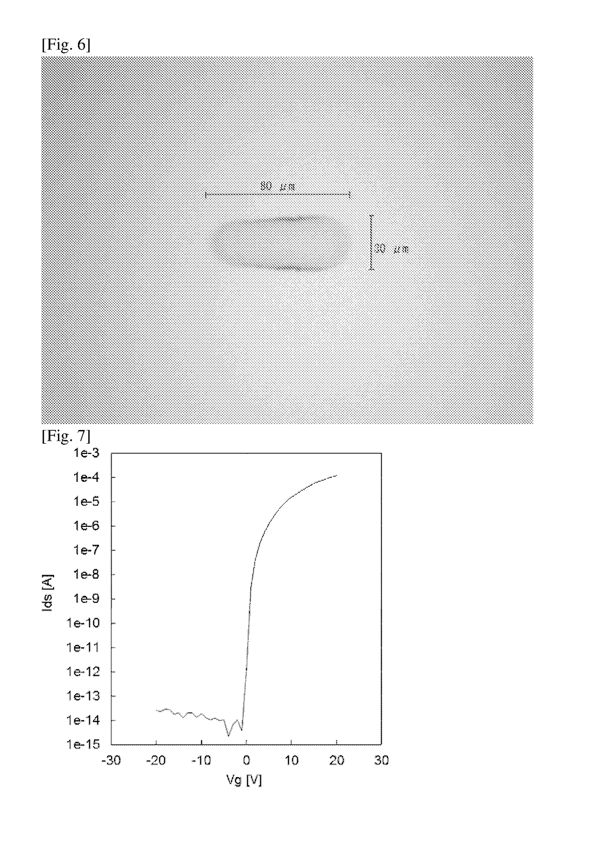
[0523]Using an inkjet device, the coating liquid 1-6 in Table 1 was ejected on a Si substrate having a thermally oxidized film (thickness: 200 nm), which had been washed with UV-ozone, to print a fine pattern. The coating liquid was favorably ejected. The substrate was dried for 10 minutes on a hotplate that had been heated to 120 degrees Celsius. The substrate was baked for 1 hour at 400 degrees Celsius in the atmosphere, to obtain an n-type oxide semiconductor film having a desired pattern as presented in FIG. 6.


PUM


Abstract

A coating liquid for forming an n-type oxide semiconductor film, the coating liquid including: a Group A element, which is at least one selected from the group consisting of Sc, Y, Ln, B, Al, and Ga; a Group B element, which is at least one of In and Tl; a Group C element, which is at least one selected from the group consisting of Group 4 elements, Group 5 elements, Group 6 elements, Group 7 elements, Group 8 elements, Group 9 elements, Group 10 elements, Group 14 elements, Group 15 elements, and Group 16 elements; and a solvent.

Description

TECHNICAL FIELD[0001]The present invention relates to a coating liquid for forming an n-type oxide semiconductor film, a method for producing an n-type oxide semiconductor film, and a method for producing a field-effect transistor.BACKGROUND ART[0002]In recent years, In—Ga—Zn—O (IGZO) n-type oxide semiconductors have been found to be semiconductors exhibiting higher carrier mobility than amorphous silicon. Thin film transistors (TFT) including these IGZO oxide semiconductors in active layers have actively been developed (see, for example, NPL 1).[0003]Typical methods for forming such oxide semiconductor thin films include the sputtering method and the laser abrasion method.[0004]However, these vacuum processes require complicated and expensive devices and involve high process cost, which is problematic. The vacuum processes have difficulties in achieving the uniform target formulation. In particular, the vacuum processes have difficulties in obtaining films where trace amounts of el...

Claims


Application Information

Patent Timeline
IPC IPC(8): H01L29/786H01L29/66H01L29/51
CPCH01L29/7869H01L29/66969H01L29/78618H01L29/517H01L29/861H01L29/24H01L21/02628H01L21/02565H01L21/02576H01L21/02581H01L21/02307H01L21/02554H01L21/28167
Inventor UEDA, NAOYUKINAKAMURA, YUKIABE, YUKIKOMATSUMOTO, SHINJISONE, YUJISAOTOME, RYOICHIARAE, SADANORIKUSAYANAGI, MINEHIDE
Owner RICOH KK
Why Eureka
Try Eureka