System and method for backside deposition of a substrate

a substrate and backside deposition technology, applied in the field of semiconductor fabrication, can solve the problems of increasing the surface stress of the wafer, reducing the size uniformity of critical features across the surface of the wafer, and new challenges for successful micro-fabrication, so as to reduce the size of features, increase the density of the device, and reduce the flatness of the wafer

Pending Publication Date: 2019-01-31
TOKYO ELECTRON LTD
View PDF10 Cites 9 Cited by
  • Summary
  • Abstract
  • Description
  • Claims
  • Application Information

AI Technical Summary

Benefits of technology

This patent is about techniques for creating a more uniform and flat surface for semiconductor devices. The challenges include distortion caused by layers of film and uneven substrate surface height caused by various fabrication steps. The patent describes a technique for depositing films on the backside of the substrate to balance stressed surfaces and reduce distortion. The technique includes a substrate holder that seals the substrate from deposition gases in the lower section of the processing chamber and provides temperature control through a separate and distinct environment above the substrate.

Problems solved by technology

The implementation of these techniques, however, has created new challenges for successful micro fabrication.
Each layer, however, adds additional stress to the surface of the wafer.
This distortion has been shown to reduce the size uniformity of critical features across the surface of the wafer.
This distortion also results in overlay errors and challenges.
If the substrate expansion is unchecked, the expansion exceeds overlay error requirements.
Moreover, if the clamping force between the substrate and the substrate chuck is insufficient to prevent substrate expansion, then the substrate can slip on the substrate chuck and larger substrate expansion will occur, resulting in larger overlay errors.
Thus, vacuum clamping is not always possible, and the weaker electrostatic clamping must be used in lieu of a vacuum clamp.
Other fabrication steps can also cause substrate expansion and contraction.
For example, deposited films can cause substrate contraction.
Also, various annealing and doping steps can create substantial amounts of bow in a given substrate.
Annealing steps can especially create overlay challenges.
The result of these various fabrication steps is a substrate that is uneven or non-planar.
With relatively significant bowing, however, it can be very difficult or impossible to accurately flatten a substrate by chucking alone.
Depositing films on the backside of a substrate is challenging.
While many different semiconductor manufacturing tools deposit films on the front side (top side or working surface) of a substrate, backside deposition is not routinely performed.
Such chucking causes scratches and defects to the backside surface.
Chucking the substrate on the front side surface will cause scratches, introduce defects, and generally destroy features under fabrication.
One solution it to apply a protective coating to the front side surface, but such a protective coating presents a new set of challenges including the application and complete removal of the protective layer without damaging the features and structures underneath.
Without physically contacting either side of the substrate, there is a challenge to properly heat the substrate for film deposition.

Method used


Image

  • System and method for backside deposition of a substrate
  • System and method for backside deposition of a substrate
  • System and method for backside deposition of a substrate

Examples


Embodiment Construction

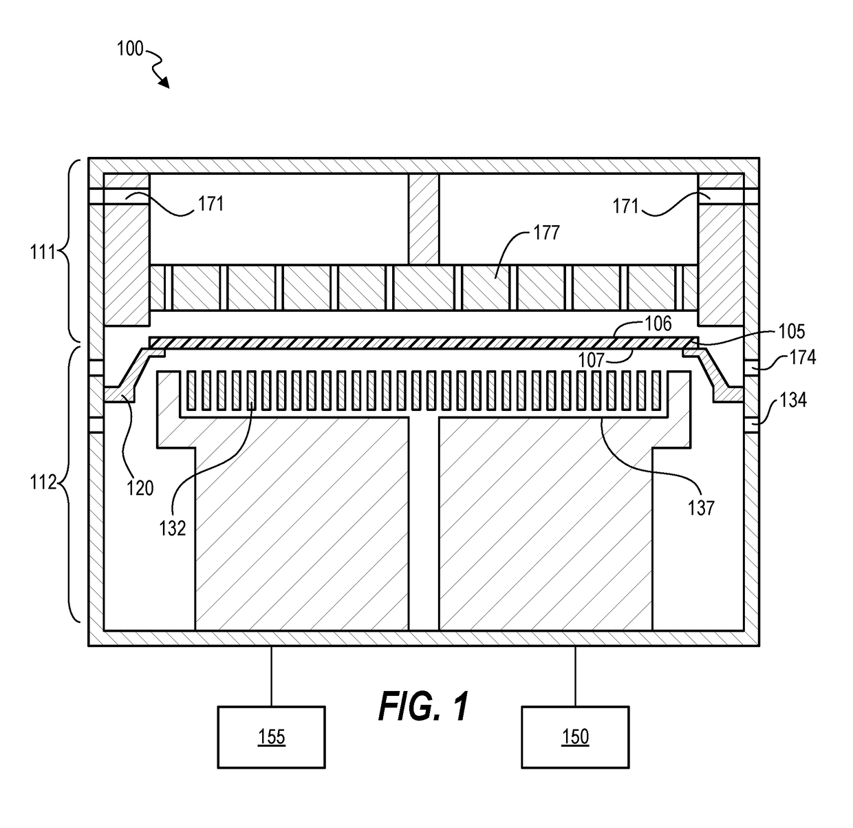
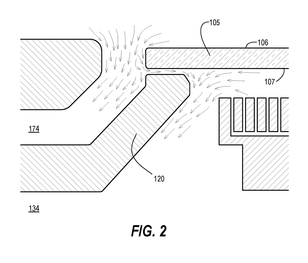
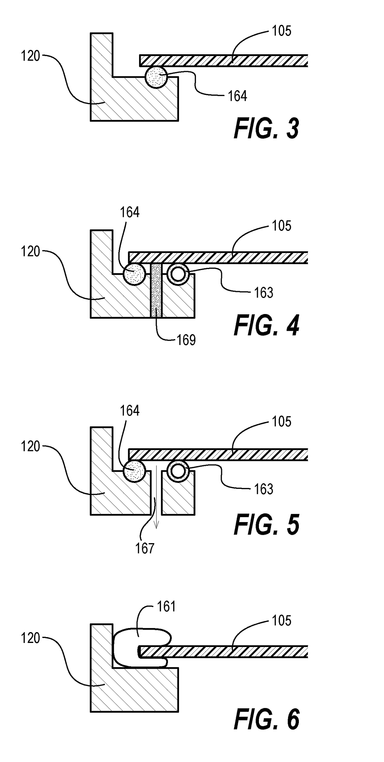
[0021]Techniques herein include a process chamber for application of thin films to backside surfaces of semiconductor substrates for the elimination or reduction of substrate flatness distortion. In other words, systems herein help make a bowed wafer flat by depositing films on the backside surfaces of wafers. The process chamber herein includes a substrate support that provides an annular perimeter seal around the bottom and / or side of the substrate which allows the majority of the substrate backside to be exposed to a process environment. One of various means of clamping and sealing the substrate can be selected. When the substrate creates a seal, the chamber is essentially bifurcated into lower and upper chambers or sections which are separate and distinct in terms of process environment. The lower section of the processing chamber includes deposition hardware configured to apply and remove thin films. The deposition hardware can be any of various types including chemical vapor d...


PUM

PropertyMeasurementUnit
Pressureaaaaaaaaaa
Flow rateaaaaaaaaaa
Heightaaaaaaaaaa

Abstract

Techniques herein include a process chamber for depositing thin films to backside surfaces of wafers to reduce wafer bowing and distortion. A substrate support provides an annular perimeter seal around the bottom and / or side of the wafer which allows the majority of the substrate backside to be exposed to a process environment. A supported wafer separates the chamber into lower and upper chambers that provide different process environments. The lower section of the processing chamber includes deposition hardware configured to apply and remove thin films. The upper section can remain a chemically inert environment, protecting the existing features on the top surface of the wafer. Multiple exhausts and differential pressures are used to prevent deposition gasses from accessing the working surface of a wafer.

Description

CROSS REFERENCE TO RELATED APPLICATIONS[0001]The present application claims the benefit of U.S. Provisional Patent Application No. 62 / 538,251, filed on Jul. 28, 2017, entitled “System and Method for Backside Deposition of a Substrate,” which is incorporated herein by reference in its entirety.BACKGROUND OF THE INVENTION[0002]This disclosure relates to semiconductor fabrication, and particularly to wafer overlay.[0003]Semiconductor fabrication involves multiple varied steps and processes. One typical process is known as photolithography (also called microlithography). Photolithography uses radiation, such as ultraviolet or visible light, to generate fine patterns in a semiconductor device design using photo-reactive films. Many types of semiconductor devices, such as diodes, transistors, and integrated circuits, can be fabricated using semiconductor fabrication techniques including photolithography, etching, film deposition, surface cleaning, metallization, and so forth.[0004]Exposur...

Claims


Application Information

Patent Timeline
IPC IPC(8): H01L21/67C23C16/455C23C16/52
CPCH01L21/67017C23C16/455C23C16/52H01L21/67126H01L21/68735C23C16/04C23C16/4409C23C16/4412C23C16/4585C23C16/4401C23C16/46H01L21/0228H01L21/02016H01L21/687H01J37/32449H01L21/67069C23C16/505
Inventor NASMAN, RONALDLEUSINK, GERRIT J.ROBISON, RODNEY L.KANG, HOYOUNGFULFORD, DANIEL
Owner TOKYO ELECTRON LTD
Why Eureka
Try Eureka