
Leadframe package with side solder ball contact and method of manufacturing

a technology of side solder ball and lead frame, which is applied in the direction of electrical equipment, semiconductor devices, semiconductor/solid-state device details, etc., can solve the problems of less resistance and lower thermal load per solder pin, and achieve the effect of less resistance, reduced thermal load and increased solder contact area

Active Publication Date: 2018-10-04
STMICROELECTRONICS SRL
View PDF0 Cites 5 Cited by
  • Summary
  • Abstract
  • Description
  • Claims
  • Application Information

AI Technical Summary

Benefits of technology

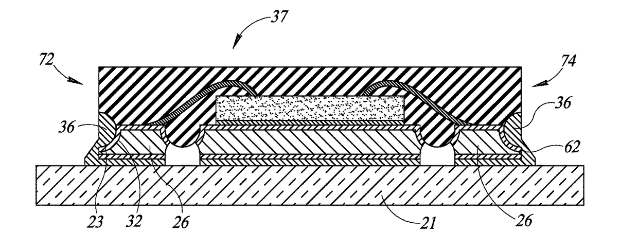
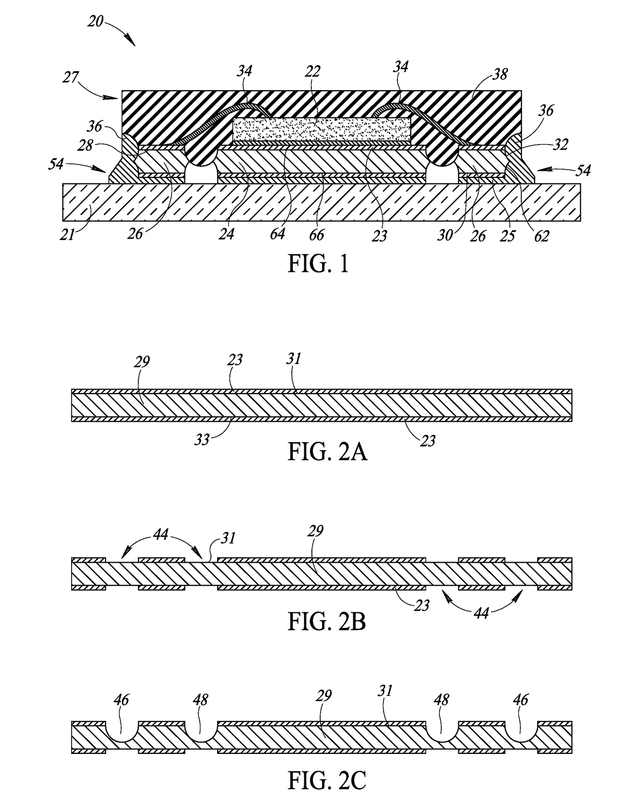
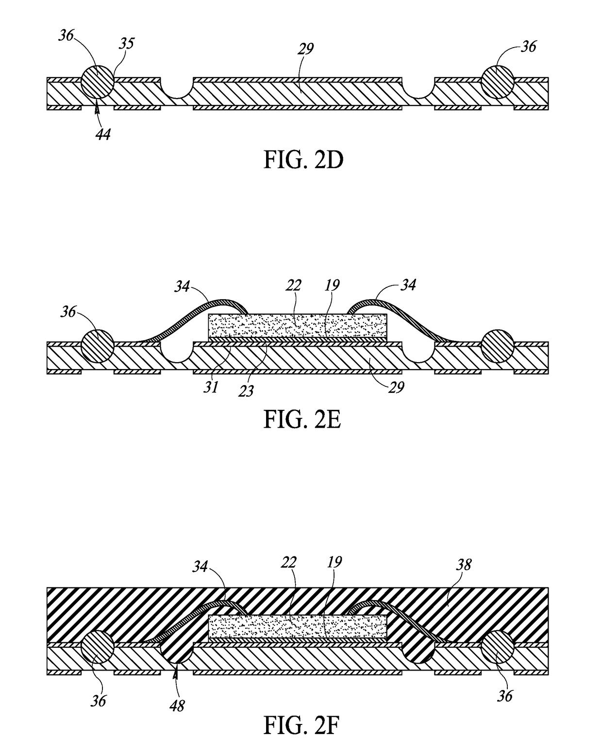
This patent describes a way to make electronic packages more efficiently. The package has a solder ball that is exposed on the side of the package and connected to the substrate when the package is attached. This makes a stronger connection and reduces the number of pins needed for power supply, saving money and allowing for more signal and data pins in the final device.

Problems solved by technology

This also increases the solder contact area between the package and the substrate, which results in less resistance and a lower thermal load per solder pin.

Method used


Image

  • Leadframe package with side solder ball contact and method of manufacturing
  • Leadframe package with side solder ball contact and method of manufacturing
  • Leadframe package with side solder ball contact and method of manufacturing

Examples


Embodiment Construction

[0014]In the following description, certain specific details are set forth in order to provide a thorough understanding of various embodiments of the disclosure. However, one skilled in the art will understand that the disclosure may be practiced without these specific details. In other instances, well-known structures associated with electronic components and fabrication techniques have not been described in detail to avoid unnecessarily obscuring the descriptions of the embodiments of the present disclosure.

[0015]Unless the context requires otherwise, throughout the specification and claims that follow, the word “comprise” and variations thereof, such as “comprises” and “comprising,” are to be construed in an open, inclusive sense, that is, as “including, but not limited to.”

[0016]The use of ordinals such as first, second and third does not necessarily imply a ranked sense of order, but rather may only distinguish between multiple instances of an act or structure.

[0017]Reference t...


PUM


Abstract

The present disclosure is directed to a leadframe package having a side solder ball contact and methods of manufacturing the same. A plurality of solder balls are coupled to recesses in a leadframe before encapsulation and singulation. After singulation, a portion of each solder ball is exposed on sidewalls of the package. This ensures that the sidewalls of the leads are solder wettable, which allows for the formation of stronger joints when the package is coupled to a substrate. This increased adhesion reduces resistance at the joints and also mitigates the effects of expansion of the components in the package such that delamination is less likely to occur. As a result, packages with a side solder ball contact have increased life cycle expectancies.

Description

BACKGROUNDTechnical Field[0001]The present disclosure is directed to a leadframe package having a side solder ball contact in order to improve solder wettability of the lead sidewall without additional post manufacturing plating.Description of the Related Art[0002]A typical leadframe package includes a die having its backside coupled to a leadframe and its active side coupled to various electrical contacts. An encapsulant is then used to cover the combined die and leadframe to create the leadframe package. The resulting combination can be connected to a circuit board, such as a printed circuit board (PCB), with solder using surface mount technology (SMT).[0003]Although SMT allows for smaller packages, it also creates some disadvantages. In particular, the solder joints between the package and the PCB can be weakened due to the PCB and the package having different coefficients of thermal expansions (CTE). Thus, the reliability of the package may, in some cases, depend on the integrit...

Claims


Application Information

Patent Timeline
Patent Type & Authority Applications(United States)
IPC IPC(8): H01L23/495H01L23/00H01L21/48H01L21/56H01L23/31H01L21/78
CPCH01L24/11H01L2224/92125H01L23/49548H01L24/27H01L24/17H01L21/78H01L21/563H01L21/4825H01L24/32H01L2224/0401H01L23/4952H01L24/46H01L21/4828H01L23/3121H01L24/09H01L24/92H01L2224/04042H01L23/3107H01L21/561H01L23/49582H01L21/4832H01L2924/181H01L2224/32245H01L2224/48091H01L2224/48247H01L2224/73265H01L24/48H01L2224/97H01L24/83H01L24/85H01L2224/2919H01L24/29H01L24/97H01L2924/00014H01L2924/00012H01L2924/00H01L2224/83H01L2224/85H01L2224/45099
Inventor TALLEDO, JEFFERSONMANGAOANG, TITO
Owner STMICROELECTRONICS SRL
Learn More