Semiconductor device
a technology of semiconductor devices and circuits, applied in field-effect transistor reliability increase, pulse technique, instruments, etc., can solve the problem that the logic circuit cannot be returned to the state before the power supply stop, and achieve the effect of enhancing the yield
- Summary
- Abstract
- Description
- Claims
- Application Information
AI Technical Summary
Benefits of technology
Problems solved by technology
Method used
Image


Examples
first embodiment
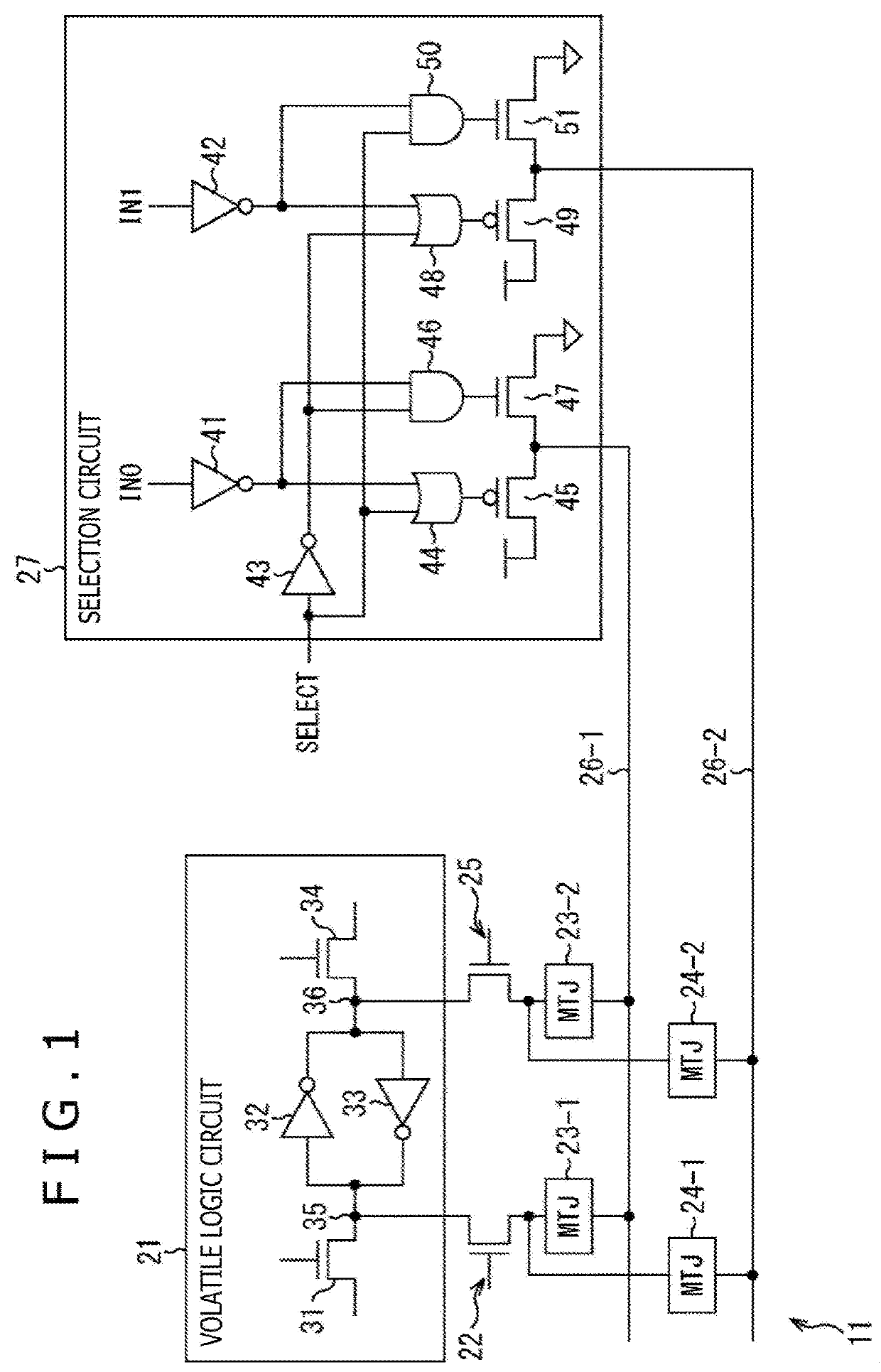
[0093]The present technology relates to a semiconductor device in which a plurality of non-volatile elements including a non-volatile element for redundancy are connected to a volatile logic circuit becoming a target of an NVPG through the same connection gate, thereby enhancing the yield at the time of manufacture.
[0094]FIG. 1 is a diagram depicting an example of a configuration of an embodiment of a semiconductor device to which the present technology is applied.
[0095]A semiconductor device 11 includes various kinds of electronic apparatuses each having a logic circuit, and devices with which these electronic apparatuses are loaded. Although, for example, the semiconductor device 11 is provided with a plurality of logic circuits or the like, in this example, only a part thereof is illustrated.
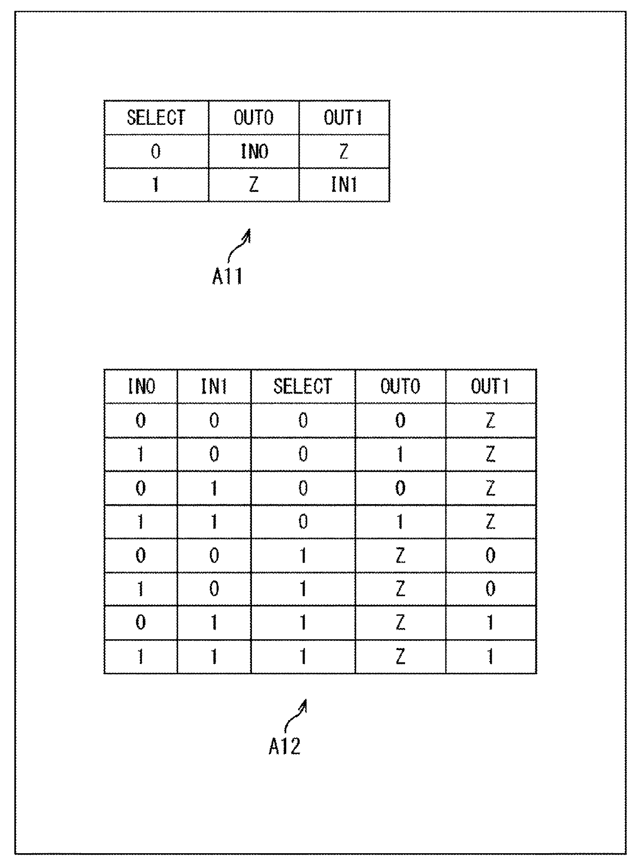
[0096]The semiconductor device 11 has a volatile logic circuit 21, a transistor 22, an MTJ (Magnetic Tunnel Junction) 23-1, an MTJ 23-2, an MTJ 24-1, an MTJ 24-2, a transistor 25, a control l...
second embodiment
[0176]Now, how the power consumption is suppressed is important in a mobile product and a wearable product including a smartphone. An LSI (Large-Scale Integration) such as a processor for controlling these products attributes to the large power consumption.
[0177]Then, a technique called PG (power gating) is known as one means for suppressing the power consumption of the LSI. A technique for stopping the supply of the power source to a block which is not operated of circuit blocks of the LSI, thereby suppressing the power consumption is known as the PG.
[0178]In addition, the power source supply control in units of smaller granularity, that is, in the units of smaller blocks, and in the units of shorter time is effective for suppressing the power consumption of the LSI. A technique which is capable of putting into practice at a flip flop level using a pair of non-volatile elements is also proposed as such a PG technique. For example, an example using the non-volatile element includes ...
third embodiment
[0367]Incidentally, WO2009 / 028298 mentioned in the second embodiment proposes the configuration in which the MTJs are added to each of the two storage nodes of the flip flop circuit (hereinafter referred to as the FF circuit) becoming the target of the NVPG through the selection transistor.
[0368]In this case, the configuration of one cell including the FF circuit, the MTJ, and the like of the non-volatile storage element, for example, is as depicted in FIG. 30.
[0369]In the example depicted in FIG. 30, a region R92 including an n-type well, and a region R93 including a p-type well are provided in a region R91 of one cell. In this example, an upper half of the region R91 in the figure is set as the region R92, and a lower half of the region R91 in the figure is set as the region R93. In a word, the region R91 is equally divided into the region R92 including the n-type well, and the region R93 including the p-type well.
[0370]An FF circuit 811 is provided on the left side of the region ...
PUM
 Abstract
Description
Claims
Application Information
 - R&D
- Intellectual Property
- Life Sciences
- Materials
- Tech Scout
- Unparalleled Data Quality
- Higher Quality Content
- 60% Fewer Hallucinations
Browse by: Latest US Patents, China's latest patents, Technical Efficacy Thesaurus, Application Domain, Technology Topic, Popular Technical Reports.
© 2025 PatSnap. All rights reserved.Legal|Privacy policy|Modern Slavery Act Transparency Statement|Sitemap|About US| Contact US: help@patsnap.com