Mask-integrated surface protective film

Active Publication Date: 2018-06-07
FURUKAWA ELECTRIC CO LTD
View PDF4 Cites 7 Cited by
  • Summary
  • Abstract
  • Description
  • Claims
  • Application Information

AI Technical Summary

Benefits of technology

The mask-integrated surface protective film described in the patent can be used in a plasma dicing method to produce semiconductor chips. It helps to protect the patterned surface of the wafer during the thinning step and ensures a good adhesion. The film is easy to peel off after the thinning step, allowing for accurate and precise chip separation using SF6 plasma. It can also be quickly removed by O2 plasma. This results in a higher yield of good quality chips.

Problems solved by technology

Further, the downsizing of the chip is required in LED or LCD driving devices and the like.
In this blade dicing method, the cutting resistance by the blade is put directly on the semiconductor wafer at the time of cutting, so that a microscopic crack (or chipping) sometimes occurs in the semiconductor chip by this cutting resistance.
Occurrence of the chipping does not only deteriorate outer appearance of the semiconductor chip, but also in some cases, there is a risk that even a circuit pattern on the chip is damaged, for example, a damage of chips is occurred due to lack (or insufficiency) of the transverse strength (or deflective strength) at the time of picking up.
Further, in the foregoing physical dicing step using such a blade, it is impossible to set the width of a kerf (also referred to as a scribe line or a street) which is an interval between chips to less than the thick blade width.
Further, a long time period to be taken for the processing of the wafer is also a problem.
However, there is a disadvantage that a wafer surface is contaminated with a sublimate at the time of cutting with a laser.
Further, the foregoing dry process has not yet led to achievement of a complete dry process.
However, the laser dicing method remains unchanged in carrying out a processing along every one line, and therefore it takes a certain time period for producing an extremely small chip.
In a case of using a wet process, such as a water-jet method of carrying out a dicing step with a water pressure, there is a possibility that a problem occurs in the material which is sensitive to a surface contamination, such as an MEMS device, a CMOS sensor, and the like.
There is also a disadvantage that narrowing of a kerf width is limited, so that a chip yield is low.
However, a transverse strength of the chip tends to be decreased by the thermal history at the time of forming the modifying layer.
Further, silicon debris sometimes occurs at the time of splitting the modifying layer by expansion.
Further, there is a risk that the collision of each adjacent chips may be bring about short (or insufficiency) of the transverse strength.
However, because singulation is performed in the backgrinding step, a phenomenon is sometimes occurred, in which an end side of the chip collides with an adjacent chip, and thereby that the chip corner is chipped.

Method used


Image

  • Mask-integrated surface protective film
  • Mask-integrated surface protective film
  • Mask-integrated surface protective film

Examples


example 1

[Example 1] Preparation of Mask-Integrated Surface Protective Film, and Production of Semiconductor Chip

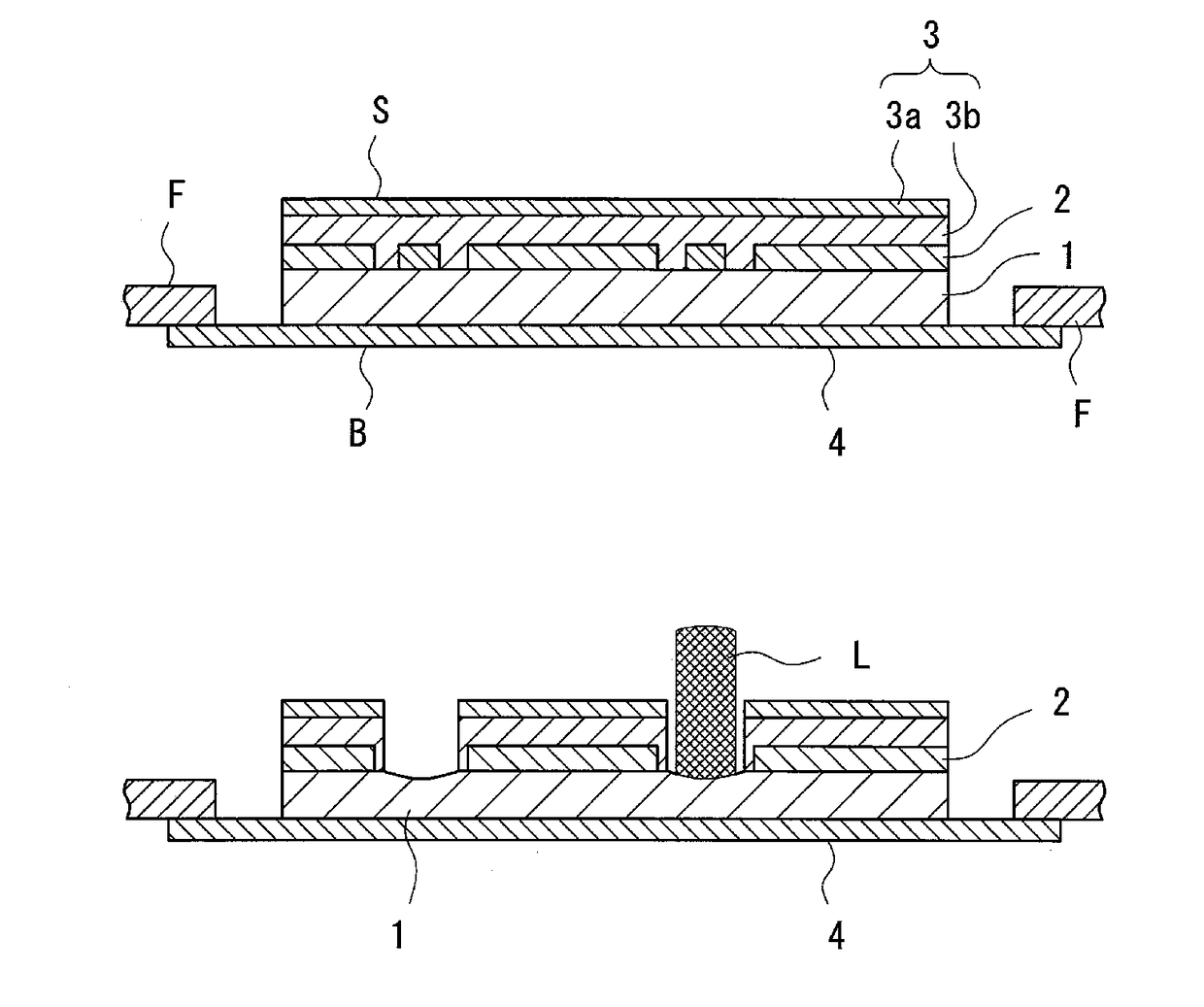
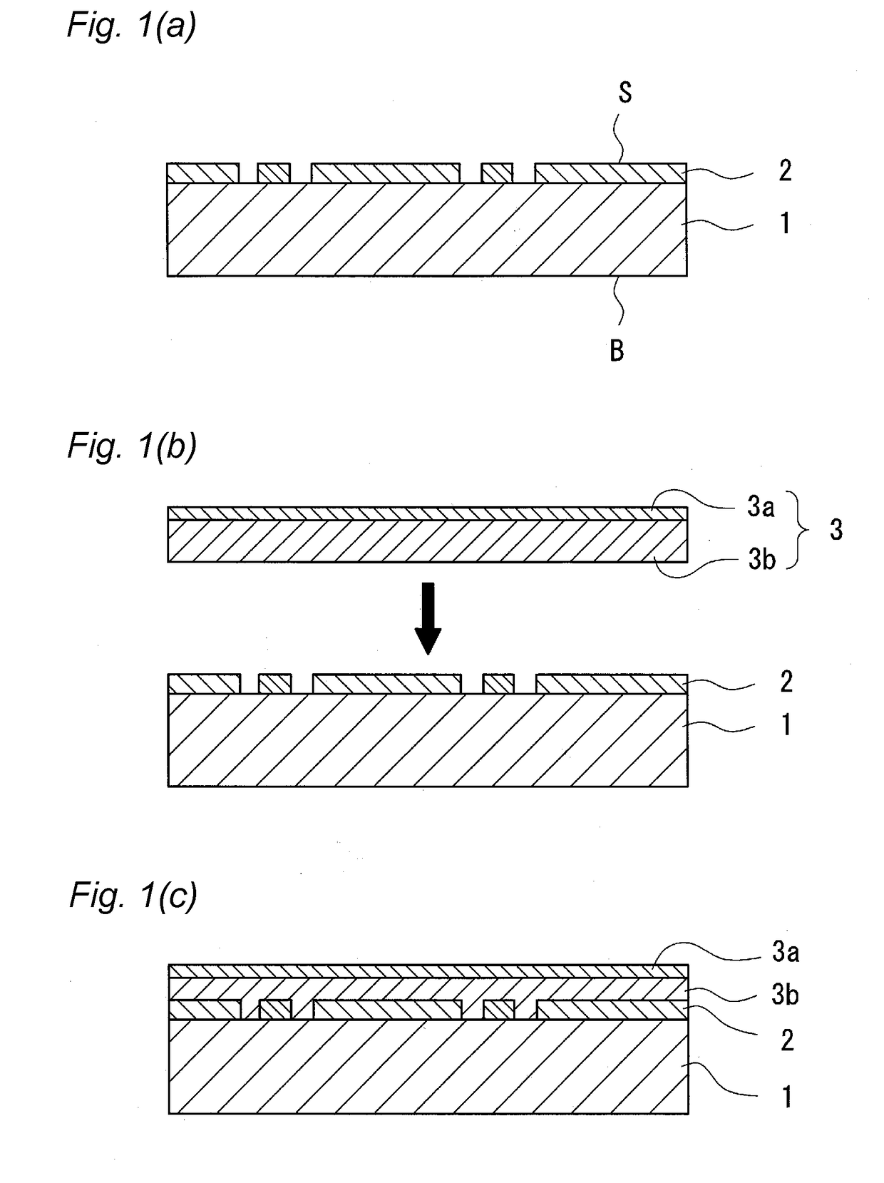
[0108]A mask-integrated surface protective film 3 composed of a polystyrene resin (trade name: XC-515, manufactured by DIC Corporation) and an ethylene-butyl acrylate copolymer (EBA) resin (trade name: LOTRYL 30BA02, manufactured by ARKEMA K.K., ethylene content rate: 70% by weight) was prepared in the form of a film in accordance with an extrusion method so that the film thicknesses of the layers were polystyrene resin: EBA resin=90 μm: 10 μm, and the total film thickness was 100 μm. Hereinafter, the polystyrene resin layer was used as the substrate film 3a, and the EBA resin layer was used as the mask material layer 3b.

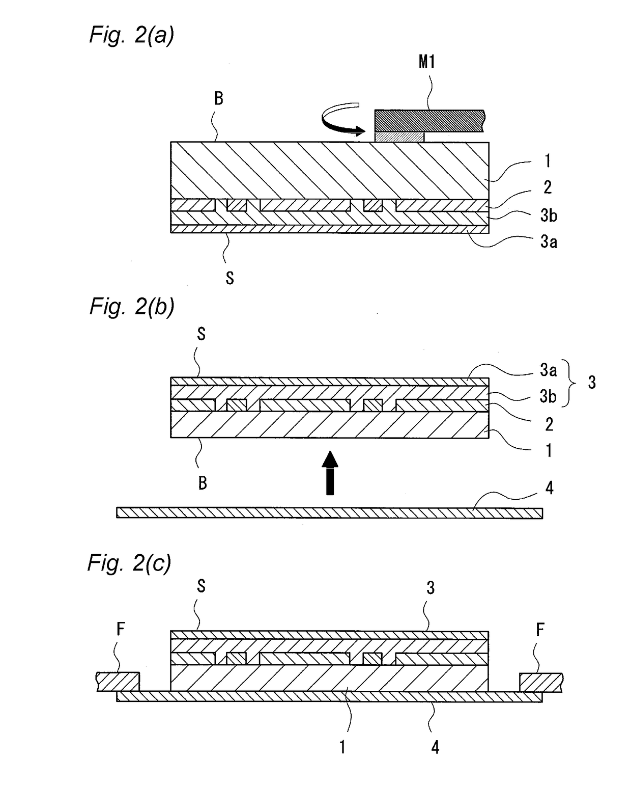
[0109]The obtained mask-integrated surface protective film was laminated on the surface of a silicon wafer (diameter: 8 inches) having thereon scribe lines using a laminator DR85001III (trade name, manufactured by Nitto Seiki Co., Ltd.). The lamination temperatur...

example 2

[Example 2] Preparation of Mask-Integrated Surface Protective Film, and Production of Semiconductor Chip

[0113]A mask-integrated surface protective film 3 composed of a polystyrene resin (trade name: XC-515, manufactured by DIC Corporation) and an ethylene-vinyl acetate copolymer (EVA) resin (trade name: ULTRATHENE 635, manufactured by Tosoh Corporation, ethylene content rate: 75% by weight) was prepared in the form of a film in accordance with an extrusion method so that the film thicknesses of the layers were polystyrene resin: EVA resin=95 μm: 5 μm, and the total film thickness was 100 μm. Hereinafter, the polystyrene resin layer was used as the substrate film 3a, and the EVA resin layer was used as the mask material layer 3b.

[0114]The obtained mask-integrated surface protective film 3 was laminated on the surface of a silicon wafer (diameter: 8 inches) having thereon scribe lines using a laminator DR85001III (trade name, manufactured by Nitto Seiki Co., Ltd.). The lamination tem...

example 3

[Example 3] Preparation of Mask-Integrated Surface Protective Film, and Production of Semiconductor Chip

[0117]A mask-integrated surface protective film 3 composed of a polystyrene resin (trade name: XC-515, manufactured by DIC Corporation) and an ethylene-vinyl acetate copolymer (EVA) resin (trade name: ULTRATHENE 750, manufactured by Tosoh Corporation, ethylene content rate: 68% by weight) was prepared in the form of a film in accordance with an extrusion method so that the film thicknesses of the layers were polystyrene resin: EVA resin=80 μm: 20 μm, and the total film thickness was 100 μm. Hereinafter, the polystyrene resin layer was used as the substrate film 3a, and the EVA resin layer was used as the mask material layer 3b.

[0118]The obtained mask-integrated surface protective film 3 was laminated on the surface of a silicon wafer (diameter: 8 inches) having thereon scribe lines using a laminator DR85001III (trade name, manufactured by Nitto Seiki Co., Ltd.). The lamination te...


PUM

PropertyMeasurementUnit
Temperatureaaaaaaaaaa
Percent by massaaaaaaaaaa

Abstract

A mask-integrated surface protective film, containing:a substrate film, anda mask material layer provided on the substrate film;wherein the mask material layer is an ethylene-vinyl acetate copolymer resin, an ethylene-methyl acrylate copolymer resin, or an ethylene-butyl acrylate copolymer resin; andwherein the thickness of the mask material layer is 50 μm or less.

Description

CROSS-REFERENCE TO RELATED APPLICATIONS[0001]This application is a Continuation of PCT International Application No. PCT / JP2016 / 082984 filed on Nov. 7, 2016, which claims priority under 35 U.S.C. § 119 (a) to Japanese Patent Application No. 2015-219735 filed in Japan on Nov. 9, 2015. Each of the above applications is hereby expressly incorporated by reference, in its entirety, into the present application.TECHNICAL FIELD[0002]The present invention relates to mask-integrated surface protective film.BACKGROUND ART[0003]In recent years, remarkable evolution has made on the thinning of the semiconductor chip and the downsizing of the chip. In particular, the thinning is required in the IC cards with built-in semiconductor IC chips, such as a memory card and a smart card. Further, the downsizing of the chip is required in LED or LCD driving devices and the like. With the increase in these demands from now, the needs for the thinning of the semiconductor chip and the downsizing of the chi...

Claims


Application Information

Patent Timeline
IPC IPC(8): H01L21/3105H01L21/304H01L21/683H01L21/3065H01L21/78H01L21/02B23K26/38
CPCH01L21/3065H01L21/31058H01L21/304H01L21/02076B23K26/38H01L21/78H01L21/6836H01L2221/68327H01L2221/6834H01L2221/68381B32B27/08B32B27/30B32B27/302B32B27/308H01L21/3086H01L21/56B32B2307/51
Inventor YOKOI, HIROTOKIUCHIYAMA, TOMOAKIOKA, YOSHIFUMI
Owner FURUKAWA ELECTRIC CO LTD
Why Eureka
Try Eureka