Silicon carbide member for plasma processing apparatus, and production method therefor
a technology of silicon carbide and plasma processing equipment, which is applied in the direction of semiconductor/solid-state device manufacturing, electric devices, basic electric elements, etc., can solve the problems of insufficient testing of the insufficient plasma resistance of -sic, and chamber contamination, so as to improve the durability of the edge ring, improve the durability, and high plasma resistance
- Summary
- Abstract
- Description
- Claims
- Application Information
AI Technical Summary
Benefits of technology
Problems solved by technology
Method used
Image

Examples
example 1
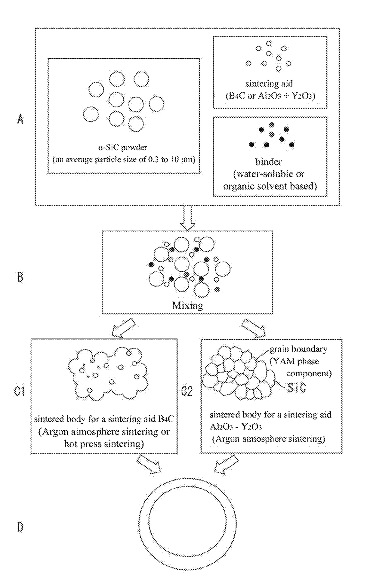
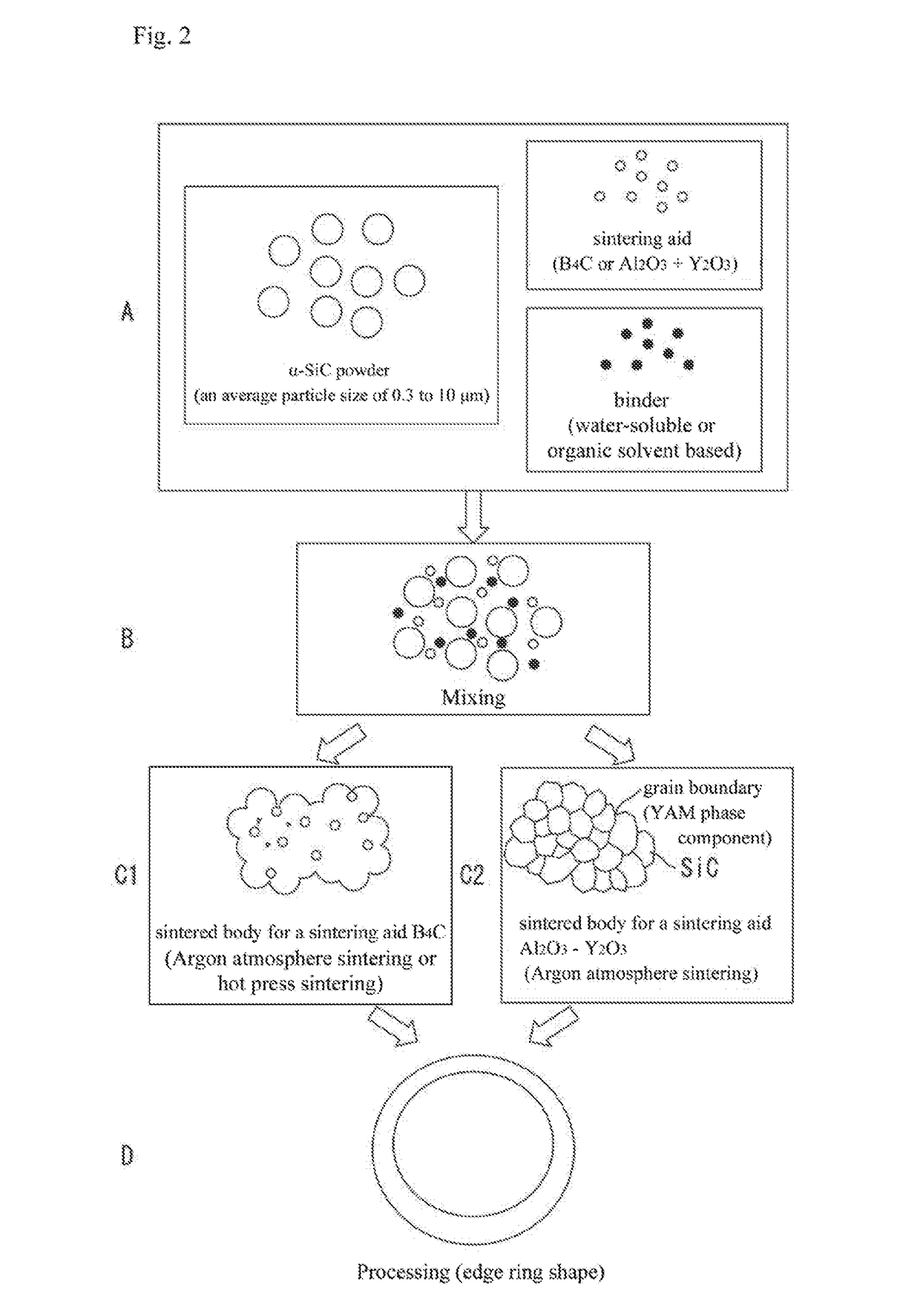
(FIG. 2A)
[0046]As a primary raw material, α-SiC particles (purity: about 98%) having an average particle size of 0.6 μm were employed, wherein the α-SiC particles was subjected to chemical cleaning to enable impurities therein, such as elements of groups IV to VIII of the 4th rows of the periodic table including iron (Fe) as a representative impurity among metal impurities, and oxides, carbides, nitrides, borides or the like of the elements, to becomes 20 ppm or less, and enable free SiO2 components to become 0.3% or less.
[0047]Then, as a sintering aid for α-SiC particles, a B4C raw material powder having a purity of 99% or more and an average particle size of 1 μm or less was prepared.
[0048]B4C as a sintering aid was added to the above α-SiC raw material powder in respective amounts of 3 weight parts, 2 weight parts and 1 weight part to prepare three types of mixed powders, and then 3 weight parts of acrylic-based water-soluble binder as a shaping aid, and pure water as a solvent,...
example 2
(FIG. 2A)
[0053]The same α-SiC raw material powder as that used in Example 1, and a fine Al2O3 powder having a purity of 99.99% or more and an average particle size of 0.5 μm as one component of the sintering aid for α-SiC were preliminarily prepared.
[0054]A fine Y2O3 powder having a purity of 99.9% or more and an average particle size of 1 μm or less as another component of the sintering aid for α-SiC was also preliminarily prepared.
[0055]Further, fine Al2O3 and Y2O3 powders each having an average particle size of 0.5 μm or less were preliminarily prepared.
[0056]3 weight parts of acrylic-based water-soluble binder as a shaping aid and pure water as a solvent were added to a mixture with respect to 100 weight parts of the mixture, wherein the mixture consists of 100 weight parts of the α-SiC raw material powder, and the Al2O3 raw material powder and the Y2O3 raw material powder each added to the α-SiC raw material powder in a respective one of amounts of 2.5 weight parts and 5 weigh...
example 3
(FIG. 2A)
[0062]B4C as a sintering aid was added to the same α-SiC raw material powder as that used in Example 1, in an amount of 1.5 weight parts to prepare a mixed powder, and then a methanol solvent was added to the mixed powder without adding any shaping aid to prepare a mixture.
(FIG. 2B)
[0063]As with Example 1, the mixture was subjected to pulverization to prepare a slurry, and the slurry was dried to prepare a shaping powder so as to prepare a 50 mm-square test piece.
(FIG. 2C1)
[0064]The test piece was sintered by hot pressing under conditions comprising a pressurizing force of 200 kg / cm2 and a temperature of 2100° C., to obtain a sintered body.
[0065]As a result of measuring the density of the obtained sintered body, it was proven that the test piece was formed as a dense sintered body having a specific gravity of 3.193 (relative density: 99.8%).
(FIG. 2D)
[0066]An edge ring having an outer diameter of about 350 mm, an inner diameter of about 295 mm, and a thickness of about 5...
PUM
| Property | Measurement | Unit |
|---|---|---|
| particle size | aaaaa | aaaaa |
| temperature | aaaaa | aaaaa |
| temperature | aaaaa | aaaaa |
Abstract
Description
Claims
Application Information
 - R&D
- Intellectual Property
- Life Sciences
- Materials
- Tech Scout
- Unparalleled Data Quality
- Higher Quality Content
- 60% Fewer Hallucinations
Browse by: Latest US Patents, China's latest patents, Technical Efficacy Thesaurus, Application Domain, Technology Topic, Popular Technical Reports.
© 2025 PatSnap. All rights reserved.Legal|Privacy policy|Modern Slavery Act Transparency Statement|Sitemap|About US| Contact US: help@patsnap.com