
ESD protection device and method for manufacturing the same

a protection device and electrostatic discharge technology, applied in the field of semiconductor devices, can solve the problems of easy damage to chips manufactured, temporary functional failure or even permanent damage to chips, etc., and achieve the effects of improving response speed, reducing junction capacitance between the induced doped region and the epitaxial semiconductor layer, and increasing junction capacitance of the esd protection devi

Active Publication Date: 2018-02-15
NANJING SILERGY SEMICON TECH CO LTD
View PDF1 Cites 12 Cited by
  • Summary
  • Abstract
  • Description
  • Claims
  • Application Information

AI Technical Summary

Benefits of technology

The patent text describes an ESD protection device and a method to improve its performance. The device includes a rectifier diode and an open-base bipolar transistor. The device has a decreased junction capacitance, which increases its response speed, by adding a second doped region around the emitter region of the open-base bipolar transistor. This additional region can be a ring-shaped region or an extension region. Overall, this invention allows for a faster and more efficient response to ESD events.

Problems solved by technology

Due to a large amount of charges being released in a short time, the energy from ESD is much higher than the bearing capacity of the chip, which may result in a temporary functional failure or even a permanent damage to the chip.
The chip having been manufactured is easily affected by ESD events between the chip and the external objects when the chip is used in various different environments.

Method used


Image

  • ESD protection device and method for manufacturing the same
  • ESD protection device and method for manufacturing the same
  • ESD protection device and method for manufacturing the same

Examples


Embodiment Construction

[0048]Exemplary embodiments of the present disclosure will be described in more details below with reference to the accompanying drawings. In the drawings, like reference numerals denote like members. The figures are not drawn to scale, for the sake of clarity. Moreover, some well-known parts may not be shown. For simplicity, the structure of the semiconductor device having been subject to several relevant process steps may be shown in one figure.

[0049]It should be understood that when one layer or region is referred to as being “above” or “on” another layer or region in the description of device structure, it can be directly above or on the other layer or region, or other layers or regions may be intervened therebetween. Moreover, if the device in the figures is turned over, the layer or region will be “under” or “below” the other layer or region.

[0050]In contrast, when one layer is referred to as being “directly on” or “on and adjacent to” or “adjoin” another layer or region, ther...


PUM


Abstract

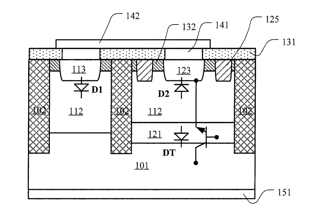
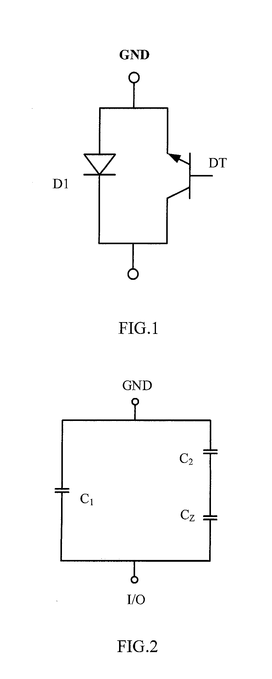
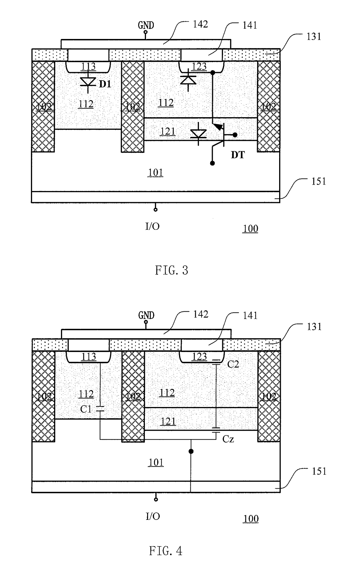
Disclosed is a method for manufacturing an ESD protection device. The ESD protection device includes a rectifier diode and an open-base bipolar transistor, the anode of the rectifier diode is the first doped region and the cathode of the rectifier diode is the semiconductor substrate, the emitter region, base region and collector region of the open-base bipolar transistor are the second doped region, the epitaxial semiconductor layer and semiconductor substrate, respectively, the first doped region and the second doped region extend through the doped region into the epitaxial semiconductor layer by a predetermined depth. The doped region can suppress the induced doped region around the second doped region, so that the parasitic capacitance of the open-base bipolar transistor is reduced and the response speed is improved.

Description

CROSS-REFERENCE TO RELATED APPLICATION[0001]This application claims the benefit of Chinese Patent Application No. 201610671655.0, filed on Aug. 15, 2016, which is incorporated herein by reference in its entirety.BACKGROUND OF THE DISCLOSUREField of the Disclosure[0002]The present disclosure relates to a semiconductor device and a method for manufacturing the same, and in particular, to an electrostatic discharge (ESD) protection device and a method for manufacturing the ESD protection device.Background of the Disclosure[0003]Electrostatic discharge (ESD) is a phenomenon that releases and transfers charges between integrated circuit chips and external objects. Due to a large amount of charges being released in a short time, the energy from ESD is much higher than the bearing capacity of the chip, which may result in a temporary functional failure or even a permanent damage to the chip. During the process for manufacturing a chip, a wrist strap or an anti-static clothing can be used t...

Claims


Application Information

Patent Timeline
Patent Type & Authority Applications(United States)
IPC IPC(8): H01L27/02H01L21/762H01L21/8222H01L21/761H01L27/06H01L29/06
CPCH01L27/0248H01L27/0664H01L29/0615H01L21/76224H01L21/8222H01L21/761H01L29/0649H01L21/77H01L27/0259H01L27/0623H01L27/0635H01L27/0761
Inventor WANG, SHIJUNYAO, FEIYIN, DENGPING
Owner NANJING SILERGY SEMICON TECH CO LTD
Learn More