Voltage control circuit and semiconductor device

a voltage control circuit and semiconductor technology, applied in the field of voltage control circuits and semiconductor devices, can solve the problems of reducing the boosted voltage, and dropping the boosted voltage generated by the booster circuit, so as to minimize the leakage current, and maintain the constant voltage

Inactive Publication Date: 2006-01-05
MONTEREY RES LLC
View PDF12 Cites 0 Cited by
  • Summary
  • Abstract
  • Description
  • Claims
  • Application Information

AI Technical Summary

Benefits of technology

[0014] Another object of the present invention is to provide a voltage control circuit capable of constantly maintaining a divided voltage for a long time and a semiconductor device having the same.
[0015] These objects of the present invention are achieved by a voltage control circuit comprising: capacitors; first switches that are respectively provided to the capacitors and selectively couple the capacitors with a given node; and second switches that are respectively provided between the first switches and the given node and selectively connect the first switches to the given node. The junction capacitances of the first and second switches that may be formed by transistors can be minimized and a potential of the given node can be constantly maintained with high precision.
[0020] The voltage control circuit may be configured so that each of the first and second switches includes a transistor having a gate that is set at a potential defined by boosting an external voltage. The gate of the reset transistor can be supplied with the boosted voltage derived from the external voltage in addition to the advantages such that the transistor junction capacitances can be further reduced and the constant voltage can be accurately controlled and maintained.
[0022] The voltage control circuit may further include a reset transistor that resets the given node in response to a reset signal, wherein the reset transistor is backward-biased in the absence of the reset signal. The leakage current can be minimized and the constant voltage can be maintained for a long time by back-biasing the gate of the reset transistor connected to the node.
[0023] The present invention includes a voltage control circuit comprising: capacitors; first switches that are respectively provided to the capacitors and selectively couple the capacitors with a given node; and a reset transistor that resets the given node in response to a reset signal, the reset transistor being back-biased in the absence of the reset signal. The leakage current can be minimized and the constant voltage can be maintained for a long time by back-biasing the gate of the reset transistor connected to the node.
[0024] The voltage control circuit may be configured so that the first switches respectively comprise first transistors having gates to which a gate voltage is applied, the gate voltage being derived from an external voltage and being higher than the external voltage. The transistor junction capacitances can be further reduced and the constant voltage can be accurately controlled and maintained. Further, the gate of the reset transistor can be supplied with the boosted voltage derived from the external voltage.

Problems solved by technology

The boosted voltage generated by the booster circuit may be dropped due to a current consumption caused in erasing or programming of a memory cell array circuit.
This means that the boosted voltage is too high and is thus subjected to a discharge operation that decreases the boosted voltage.
Therefore, it is very difficult to make the boosted voltage VPP equal to the target voltage.
This makes it difficult for the conventional voltage control circuit to control and maintain the constant voltage with a precision equal to mV.
Thus, the boosted voltage VPP cannot be controlled precisely.
This makes it difficult to constantly maintain the divided voltage for a long time.

Method used


Image

  • Voltage control circuit and semiconductor device
  • Voltage control circuit and semiconductor device
  • Voltage control circuit and semiconductor device

Examples


Embodiment Construction

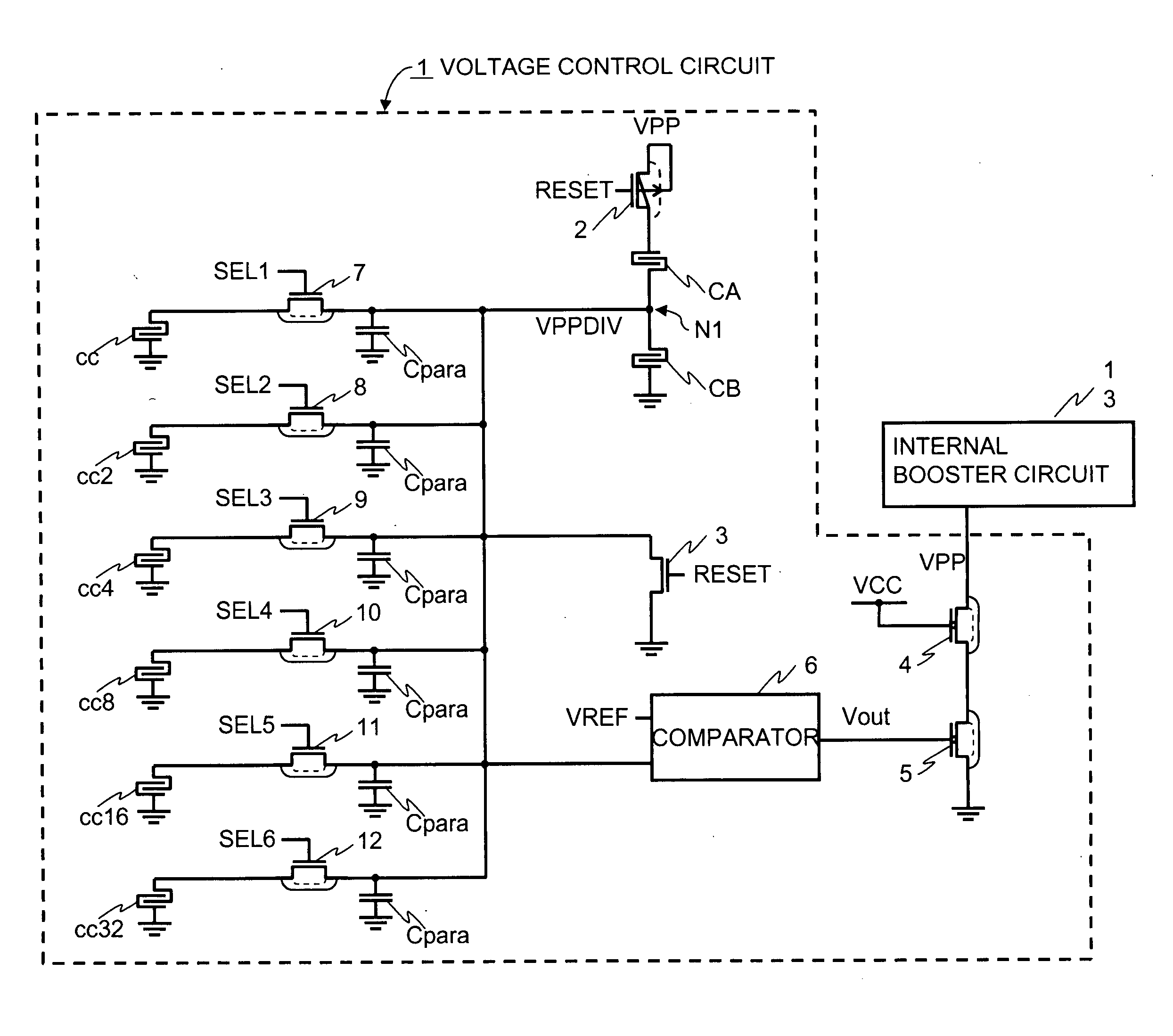
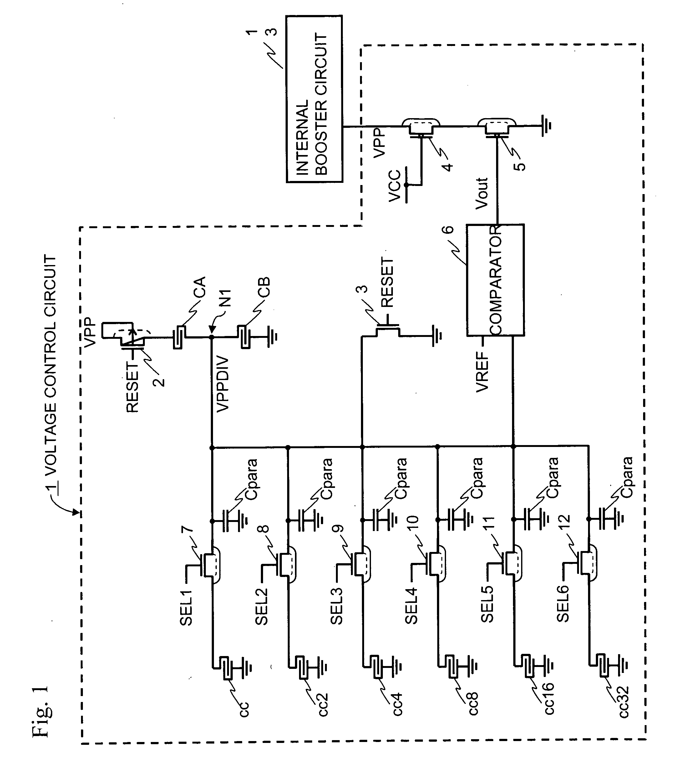
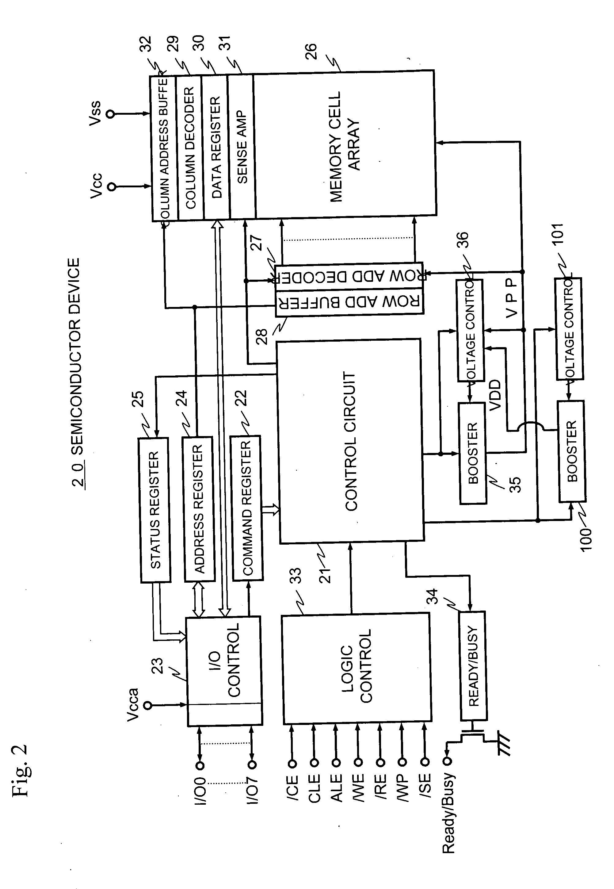
[0040]FIG. 2 is a block diagram of an outline of a semiconductor device according to an embodiment of the present invention. A semiconductor device 20 includes a control circuit 21, a command register 22, an I / O control circuit 23, an address register 24, a status register 25, a memory cell array 26, a row address decoder 27, a row address buffer 28, a column decoder 29, a data register 30, a sense amplifier 31, a column address buffer 32, a logic controller 33, and a ready / busy register 34, an internal booster circuit 35, a voltage control circuit 36, an internal booster circuit 100, and a voltage control circuit 101.

[0041] The semiconductor device 20 may be solely packaged into a semiconductor memory device such as a flash memory, or may be incorporated as a part of the semiconductor device such as a system LSI. The logic controller 33 externally receives control signals such as a chip enable signal / CE, a command latch enable signal CLE, an address latch enable signal ALE, a wri...


PUM


Abstract

A voltage control circuit includes capacitors, first switches that are respectively provided to the capacitors and selectively couple the capacitors with a given node, and second switches that are respectively provided between the first switches and the given node and selectively connect the first switches to the given node.

Description

CROSS REFERENCE TO RELATED APPLICATIONS [0001] This is a continuation of International Application No. PCT / JP2004 / 008997, filed Jun. 25, 2004.BACKGROUND OF THE INVENTION [0002] 1. Field of the Invention [0003] The present invention relates to a voltage control circuit and a semiconductor device. More particularly, the present invention relates to a voltage control circuit capable of precisely controlling a target to a constant voltage and a semiconductor device including the same. [0004] 2. Description of the Related Art [0005] A non-volatile semiconductor memory device operates so that data is written by a programming operation in which a charge is injected into a gate of a memory cell transistor, and is erased by an erase operation in which the charge is removed from the gate. In programming and erasing, the gate, drain and source of the memory cell transistor are supplied with voltages based on operations. [0006] Generally, the injecting of the charge into the gate and the removi...

Claims


Application Information

Patent Timeline
IPC IPC(8): G11C7/00
CPCG11C5/14H02M3/07G11C16/30
Inventor YAMADA, SHIGEKAZU
Owner MONTEREY RES LLC
Why Eureka
Try Eureka