Multi-Layer Ceramic Capacitor and Method of Producing the Same
- Summary
- Abstract
- Description
- Claims
- Application Information
AI Technical Summary
Benefits of technology
Problems solved by technology
Method used
Image

Examples
first embodiment
1. First Embodiment
[0054]1.1 Overall Configuration of Multi-Layer Ceramic Capacitor 10
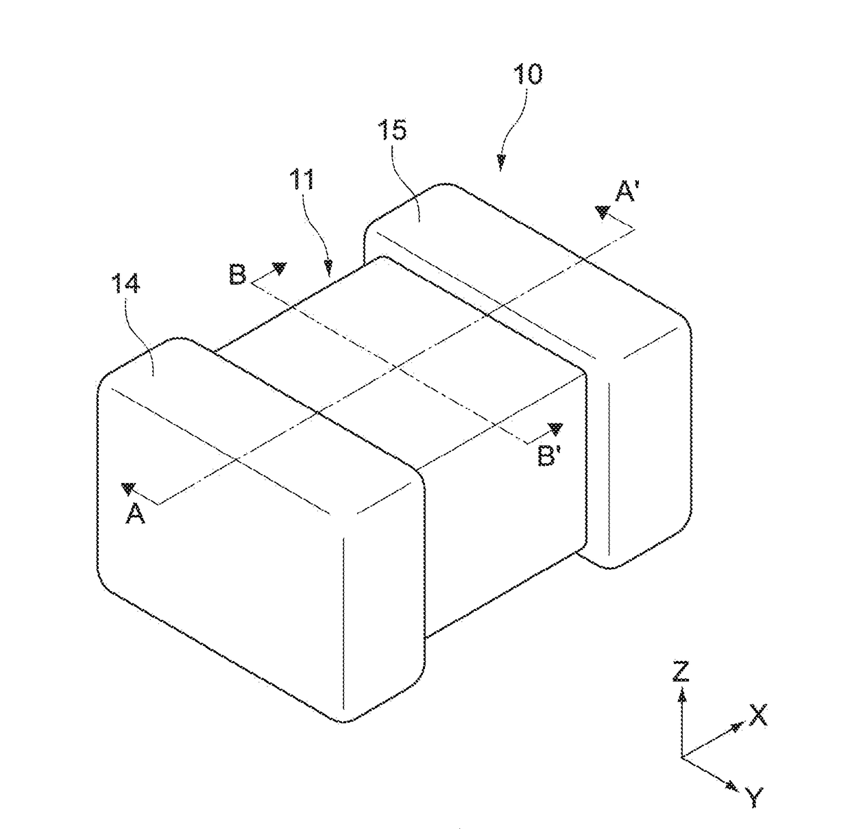
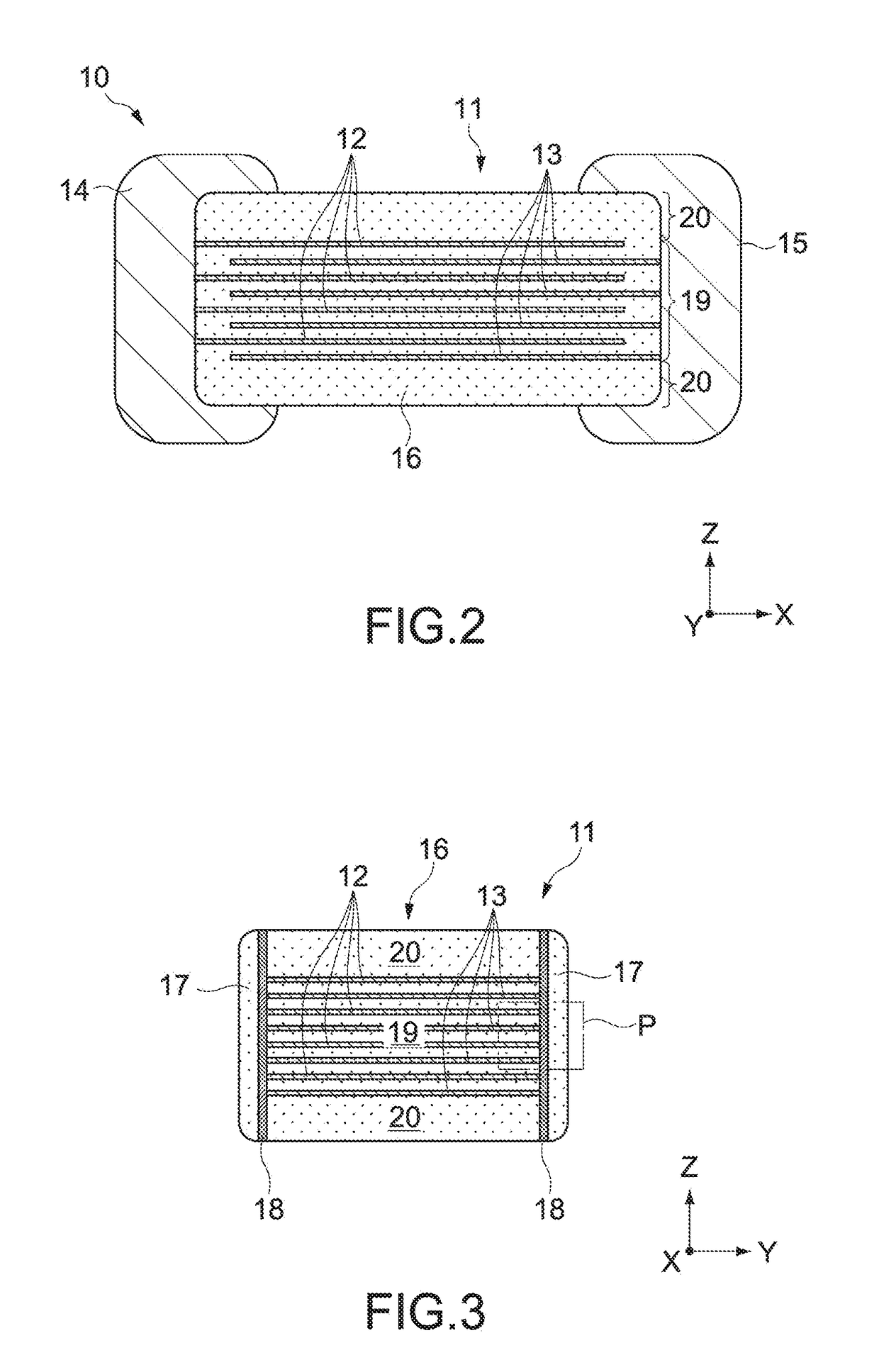
[0055]FIGS. 1 to 3 each show a multi-layer ceramic capacitor 10 according to a first embodiment of the present invention. FIG. 1 is a perspective view of the multi-layer ceramic capacitor 10. FIG. 2 is a cross-sectional view of the multi-layer ceramic capacitor 10 taken along the A-A′ line in FIG. 1. FIG. 3 is a cross-sectional view of the multi-layer ceramic capacitor 10 taken along the B-B′ line in FIG. 1.
[0056]The multi-layer ceramic capacitor 10 includes a body 11, a first external electrode 14, and a second external electrode 15.
[0057]Typically, the body 11 has two side surfaces oriented in a Y-axis direction and two main surfaces oriented in a Z-axis direction. Ridges connecting the respective surfaces of the body 11 are chamfered. It should be noted that the form of the body 11 is not limited to the form as described above. For example, the surfaces of the body 11 may be curved surfaces, and...
second embodiment
2. Second Embodiment
[0155]A second embodiment of the present invention will be described. Hereinafter, configurations similar to those of the first embodiment will be denoted by similar symbols, and detailed description thereof will be omitted.
[0156]In the first embodiment, the unsintered body 111 is produced by attaching the sheet-shaped bonding units 118 and side margins 117 to the unsintered multi-layer chip 116. As a result, as shown in FIG. 10, the unsintered body 111 includes ridge lines (where two different surfaces intersect with each other) and corners (where three different surfaces intersect with one another). The ridge lines and the corners connect the surfaces of the body 111 to one another.
[0157]When the body 111 includes the ridge lines and the corners, due to collision of the bodies 111 with one another in the production process, chipping or cracking is generated in the bodies 111. Thus, in order to suppress generation of such chipping or cracking, the ridge lines an...
PUM
| Property | Measurement | Unit |
|---|---|---|
| Thickness | aaaaa | aaaaa |
| Diameter | aaaaa | aaaaa |
Abstract
Description
Claims
Application Information
 - R&D
- Intellectual Property
- Life Sciences
- Materials
- Tech Scout
- Unparalleled Data Quality
- Higher Quality Content
- 60% Fewer Hallucinations
Browse by: Latest US Patents, China's latest patents, Technical Efficacy Thesaurus, Application Domain, Technology Topic, Popular Technical Reports.
© 2025 PatSnap. All rights reserved.Legal|Privacy policy|Modern Slavery Act Transparency Statement|Sitemap|About US| Contact US: help@patsnap.com