Photovoltaic cells

a photovoltaic cell and photovoltaic technology, applied in the field of photovoltaic cells, can solve the problems of high conductivity of graphene, non-linear optical crystals, bulky and expensive, etc., and achieve the effects of dramatic enhancement of local electric fields, increased signal strength, and increased cell signal strength

Inactive Publication Date: 2017-06-22
UNIV OF MANCHESTER
View PDF7 Cites 7 Cited by
  • Summary
  • Abstract
  • Description
  • Claims
  • Application Information

AI Technical Summary

Benefits of technology

[0033]In an embodiment, the first electrode layer comprises graphene. In an alternative embodiment, the first electrode layer comprises modified graphene (e.g. doped graphene). Graphene is both an excellent conductor and is substantially transparent to actinic radiation, e.g. visible and near visible light. Graphene is also very flexible. Many of its derivatives (e.g. doped graphene) retain these properties. Graphene also has a variable work function which can be changed easily using electrostatic gating.
[0105]This method of making a thin film of a transition metal dichalcogenides is known as chemical exfoliation. It is a cheap and easy method for manufacturing thin films of materials in large quantities. A further benefit of using transition metal dichalcogenides (and particularly WS2) in the photovoltaic cells of the invention is that this method of manufacture can be used and the cost of the photovoltaic cells made by this invention can be expected to be considerably lower than the photovoltaic cells currently available (or at least those with energy conversion efficiencies which are comparable to the cells of the present invention) as a result.

Problems solved by technology

It is sometimes called “insulating graphite” and it might be used in instances where graphene's high conductivity is a disadvantage (ultra-thin, high quality, insulating layers for nano-electronics, non-conductive, ultra-strong, composite materials).
However, there is still a large number of other layered materials which potentially can be cleaved and prepared as monolayers.
Despite great progress in optical disciplines, active optics still relies heavily on either liquid crystals, which guarantee deep modulation in inexpensive and small cells, but are quite slow, or non-linear optical crystals, which are fast, but bulky and expensive.

Method used


Image

  • Photovoltaic cells
  • Photovoltaic cells
  • Photovoltaic cells

Examples


example 2

on of a Device of the Invention Using Solution Processed Materials

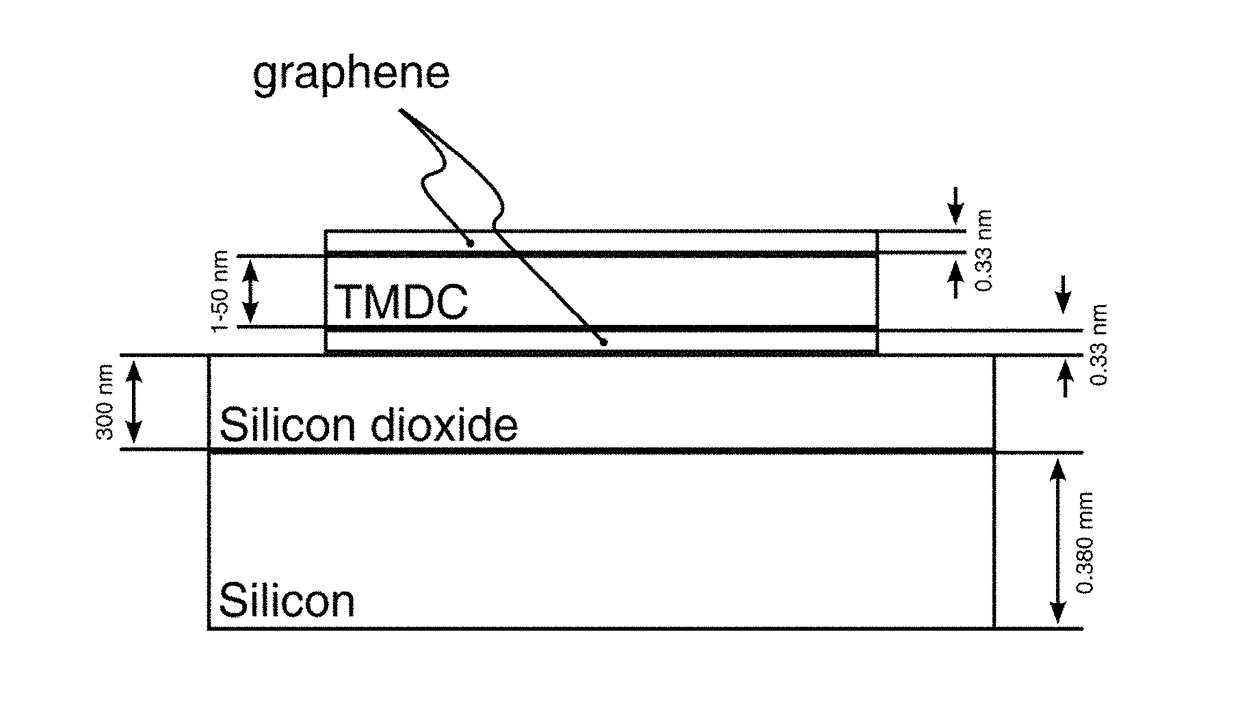
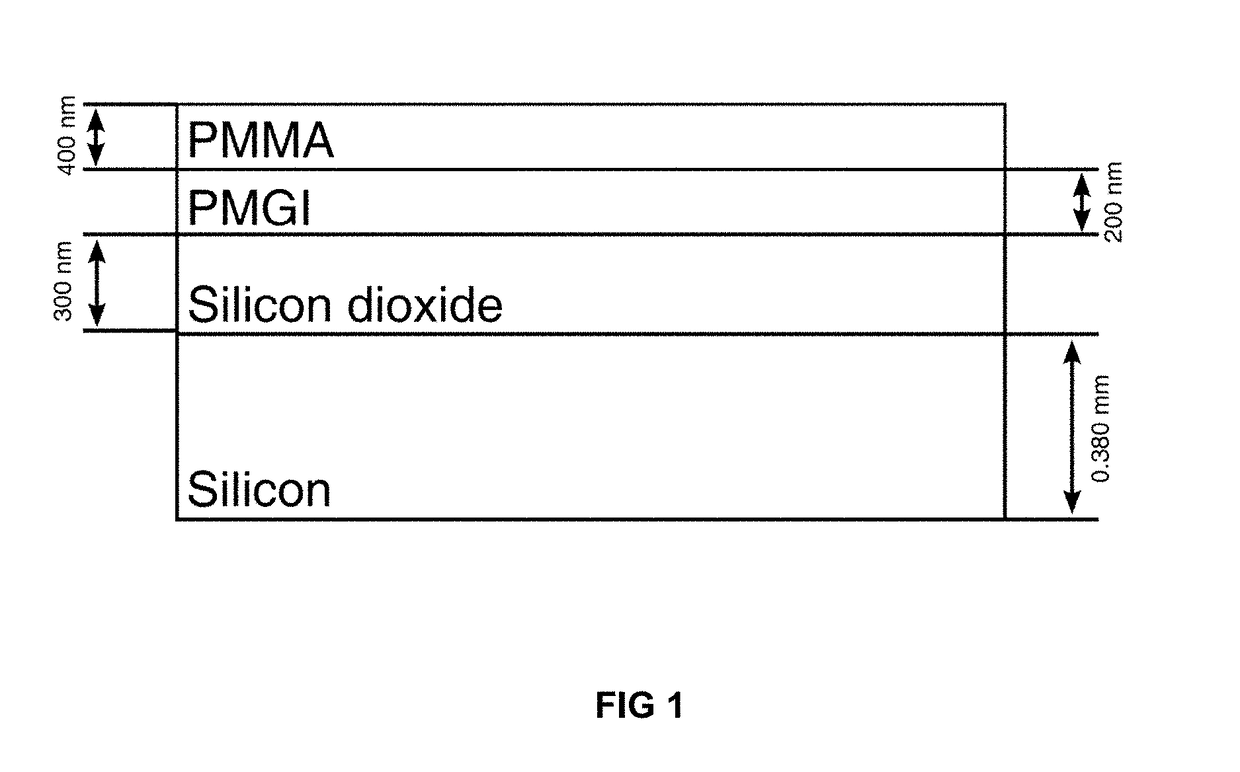
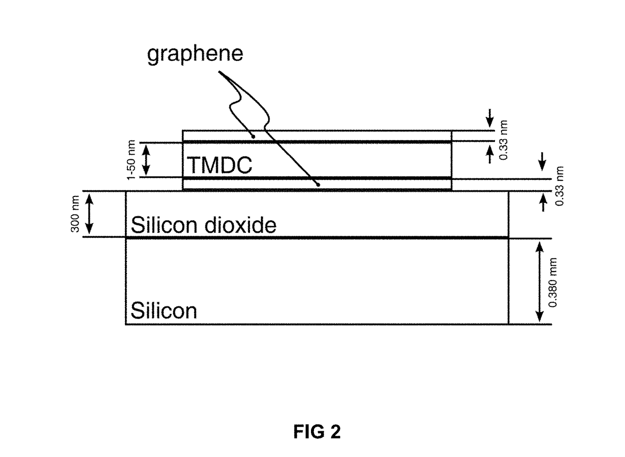
[0202]An alternative exemplary method of preparing the devices, cells and heterostructures according to the invention is as follows.[0203]1. Metal electrodes (Cr / Au (5 / 50 nm) in our case) are patterned onto a substrate (in this case silicon / silicon dioxide).[0204]2. A WS2 film is prepared as follows.[0205]a. WS2 powder is put into a 35% ethanol / water mixture and placed in an ultrasonic bath for 5 days to break up the WS2 crystals to few layer nanoplatlets which form a suspension.[0206]b. The suspension is filtered through a cellulose membrane and a film is left, attached to the filter.[0207]c. By dipping the membrane in water, a thin film (˜50 nm thick) delaminates from the WS2 film and is left floating on the water's surface.[0208]3. The membrane can be ‘fished’ from the water with the gold patterned substrate so that the WS2 film covers many metal electrodes.[0209]4. CVD graphene can then be transferred as previousl...

example 3

on of a Flexible Device

[0211]A device as prepared in Example 1 was transferred to a PET (poly(ethylene terephthalate)) substrate and subjected to strain. As the device was put under strain, it's performance as a transistor was measured and it was found that there was no change of the current with a strain of up to about 5%. It was also shown that it is still possible to modulate the current when the device is under strain.

After it was subjected to strain, the photovoltaic properties of the device were tested as for the Si / SiO2 device described above.

[0212]The inset of FIG. 7 shows the photocurrent of the flexible device (inset, as crossed squares) after it has been placed under strain measured with a 1.95 eV laser as a function of intensity and follows a sublinear dependence.

[0213]In general, the EQE in our devices on Si / SiO2 substrate is somewhat higher in comparison with the flexible PET devices due to multiple reflections in SiO2 which effectively works as a cavity and increases ...

example 5

on and Photovoltaic Ability of Devices Incorporating Gold Nanostructures

[0215]Two devices which incorporate a gold nanostructure were prepared:

A) A 1 nm thick gold film was thermally evaporated onto a pre-existing graphene / WS / graphene device which had previously been seen to exhibit a photovoltaic signal (the device of Example 1). The nanostructures in this case are self-forming as the gold (in the form of Cr / Au (5 / 50 nm)) does not make a continuous layer but instead forms islands. The signal was seen to increase by a factor of up to 15 following this procedure (FIG. 8).

B) A second device type was made (according to the method described in Example 1) in which the photoactive part of the device had two regions: one area where nanostructures were fabricated and one without. The structures are patterned using lithographic techniques. In this case the gold (in the form of Cr / Au (5 / 50 nm)) dots (disks) have a diameter of 150 nm and a pitch of 350 nm. The average photocurrent was greatly ...


PUM

PropertyMeasurementUnit
thickaaaaaaaaaa
diameteraaaaaaaaaa
diameteraaaaaaaaaa

Abstract

This invention relates to cells and devices for harvesting light. Specifically the cell comprises at least one electrode which comprises graphene or modified graphene and layer of a transition metal dichalcogenide in a vertical heterostructure. The cell may be part of a light harvesting device. The invention also relates to materials and methods for making such cells and devices.

Description

[0001]This invention relates to cells and devices for harvesting light. Specifically the cell comprises at least one electrode which comprises graphene or modified graphene and layer of a transition metal dichalcogenide in a vertical heterostructure. The cell may be part of a light harvesting device. The invention also relates to materials and methods for making such cells and devices.BACKGROUND[0002]Graphene is a two-dimensional allotrope of carbon, in which a planar sheet of sp2 hybridised carbon atoms is arranged in a ‘honeycomb pattern’ of tessellated hexagons. Essentially graphene is a single layer of graphite. Graphene is a semi metal with high room temperature charge carrier mobility. It is stable in ambient conditions and its electronic properties can be controlled through application of an electric field as with traditional silicon transistors (K. S. Novoselov, A. K. Geim, S. V. Morozov, D. Jiang, Y. Zhang, S. V. Dubonos, I. V. Grigorieva and A. A. Firsov, “Electric field E...

Claims


Application Information

Patent Timeline
Patent Type & Authority Applications(United States)
IPC IPC(8): H01L31/032H01L31/18H01L31/0352H01L31/0224
CPCH01L31/032H01L31/035209H01L31/18H01L31/022425B82Y30/00H01L31/022466H01L31/1884Y02E10/50H01L31/022433H01L31/186
Inventor NOVOSELOV, KONSTANTINBRITNELL, LIAM
Owner UNIV OF MANCHESTER
Why Eureka
Try Eureka