Metal nanowire having core-shell structure coated with graphene, and manufacturing method therefor
a technology of graphene and copper nanowires, which is applied in the direction of metal/alloy conductors, conductors, transportation and packaging, etc., can solve the problems of silver nanowires, difficult to apply ito to flexible electric devices, and increasing concern about the amount of indium tin oxide present on earth, etc., to achieve excellent optical, electrical and mechanical properties, and high manufacturing efficiency. , the effect of improving the chemical vapor deposition
- Summary
- Abstract
- Description
- Claims
- Application Information
AI Technical Summary
Benefits of technology
Problems solved by technology
Method used
Image
Examples
fabrication example 1
Fabrication of a Transparent Electrode Film
[0065]A solution was prepared by mixing 37 ml of acetone, 38 ml of ethanol, 17 ml of ethyl acetate, 12 ml of isopropanol and 20 ml of toluene. 5 mg of the copper nanowire (CuNW-G) coated on the surface with graphene which was fabricated in Example 1 was added to 10 ml of the solution. Then, CuNW-G was dispersed by ultrasonic treatment to prepare an ink formulation. 0.3 ml of the ink formulation was applied onto a glass substrate (3×3 cm2) in a manner of spray-coating. Subsequently, a uniform pressure of 24 MPa was applied to the substrate, and annealing treatment was performed at 300° C. in the Ar atmosphere for one hour to form a nanowire layer having a copper-graphene core-shell structure, thereby producing a transparent electrode film.
fabrication examples 2 to 4
[0066]A transparent electrode film was fabricated in the same manner as in Fabrication Example 1, except that the ink formulation in which CuNW-G was dispersed was used in the amounts shown in Table 1 below.
experimental example 1
Measurement of Light Transmittance and Sheet Resistance
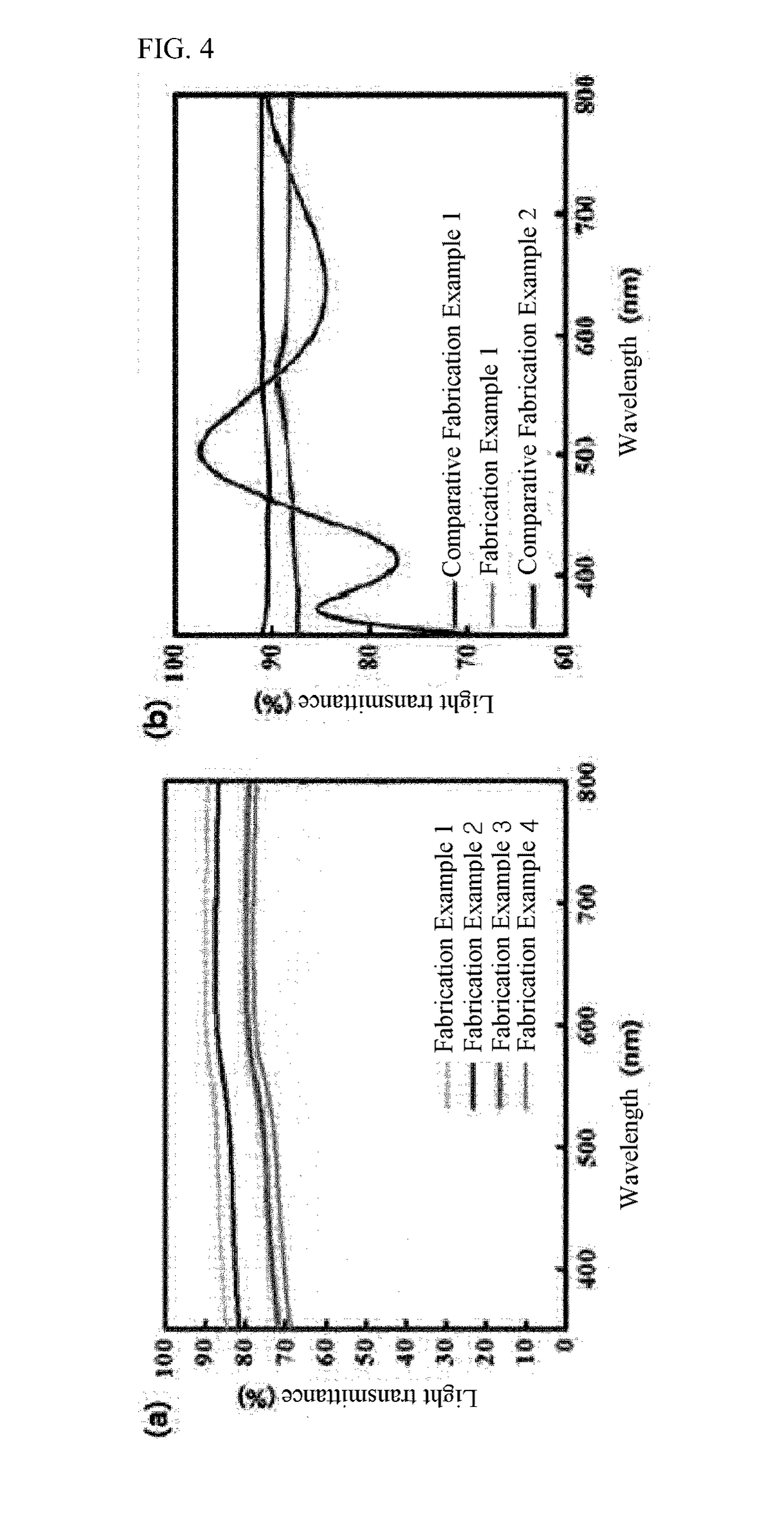
[0069]The light transmittances and sheet resistances of the transparent electrodes produced in Fabrication Examples 1 to 4 were measured using UV / Vis spectroscopy and a 4-point probe. The results are shown in Table 1 and FIG. 4 below.
TABLE 1LightSheetInk formulationtransmittanceresistance(ml)(%) at 550 nm(Ω / sq)Fabrication Example0.388.3115.21Fabrication Example0.785.350.72Fabrication Example1.077.438.03Fabrication Example1.574.928.94
[0070]FIG. 4(b) shows that the CuNW-G transparent electrode of Fabrication Example 1 and the CuNW transparent electrode of Comparative Fabrication Example 1 have a higher light transmittance in the visible light region than the ITO transparent electrode of Comparative Fabrication Example 2. In addition, the CuNW-G transparent electrodes of Fabrication Examples 1 to 4 have an almost constant light transmittance in the near infrared region. This means that the CuNW-G transparent electrodes of Fabricati...
PUM
| Property | Measurement | Unit |
|---|---|---|
| Temperature | aaaaa | aaaaa |
| Temperature | aaaaa | aaaaa |
| Length | aaaaa | aaaaa |
Abstract
Description
Claims
Application Information
 - R&D Engineer
- R&D Manager
- IP Professional
- Industry Leading Data Capabilities
- Powerful AI technology
- Patent DNA Extraction
Browse by: Latest US Patents, China's latest patents, Technical Efficacy Thesaurus, Application Domain, Technology Topic, Popular Technical Reports.
© 2024 PatSnap. All rights reserved.Legal|Privacy policy|Modern Slavery Act Transparency Statement|Sitemap|About US| Contact US: help@patsnap.com


