
Porous silicon relaxation medium for dislocation free CMOS devices

a relaxation medium and porous silicon technology, applied in the field of semiconductor processing, can solve the problems of forming a dually strained channel (tensile for nfet and compressive for pfet), and achieve the effect of reducing the number of strained channels

Inactive Publication Date: 2017-01-05
ELPIS TECH INC
View PDF0 Cites 12 Cited by
  • Summary
  • Abstract
  • Description
  • Claims
  • Application Information

AI Technical Summary

Benefits of technology

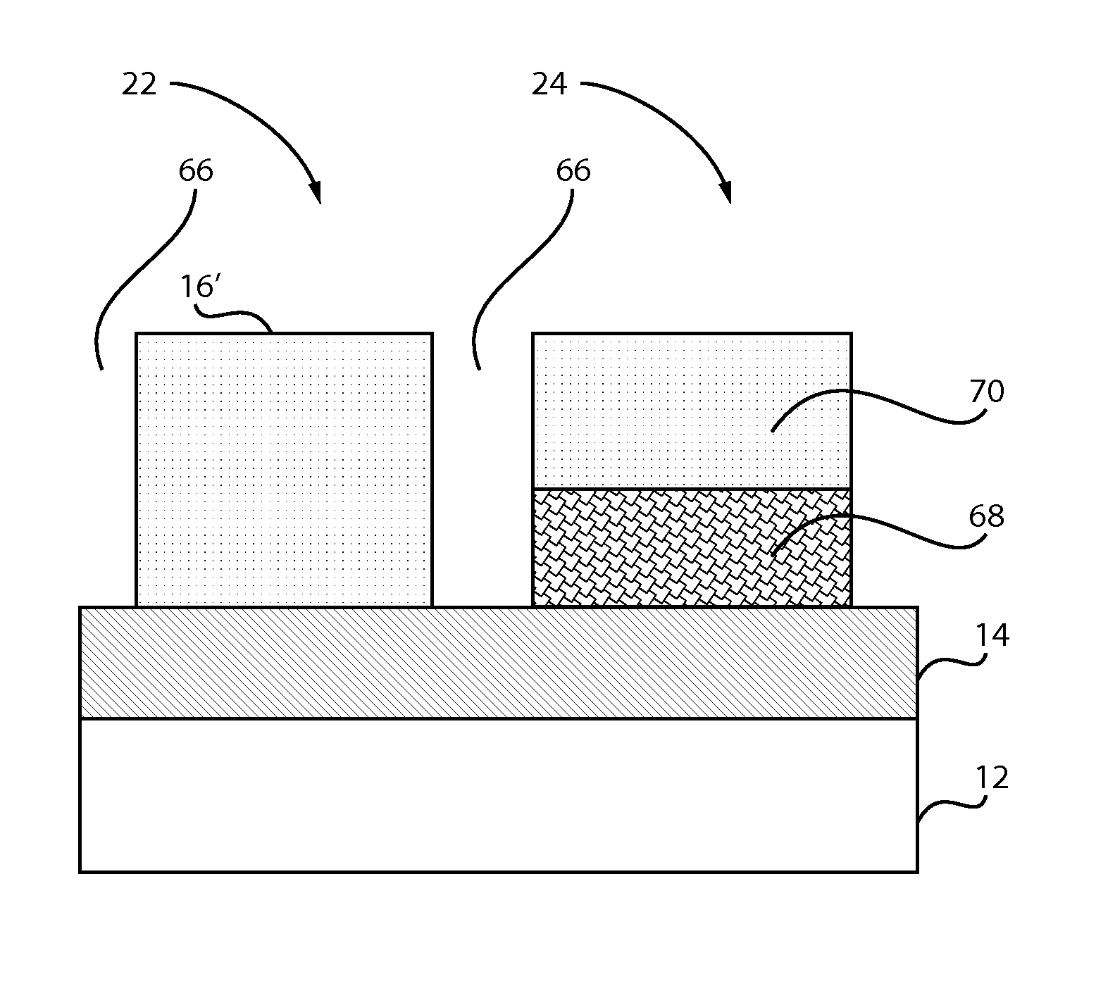
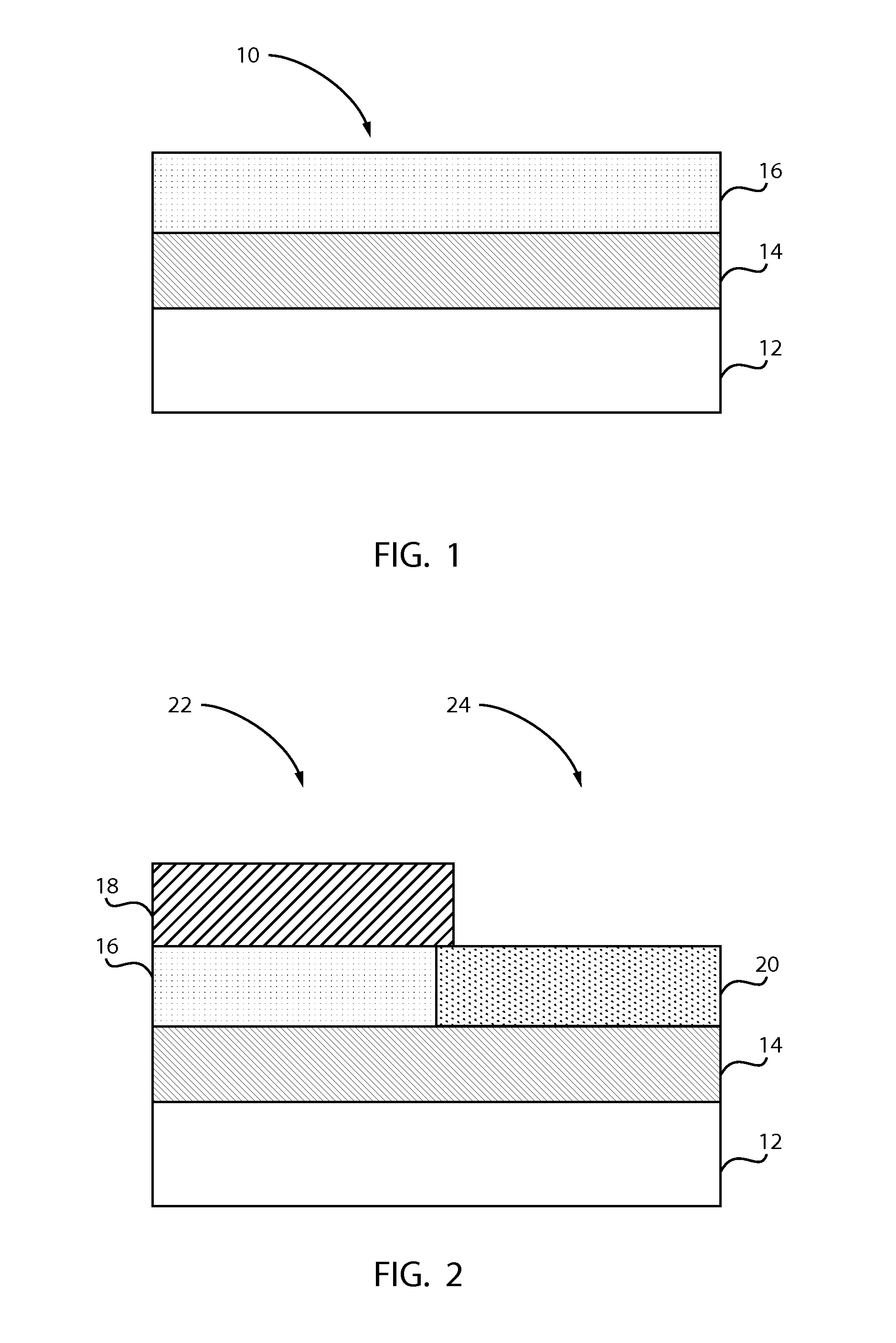
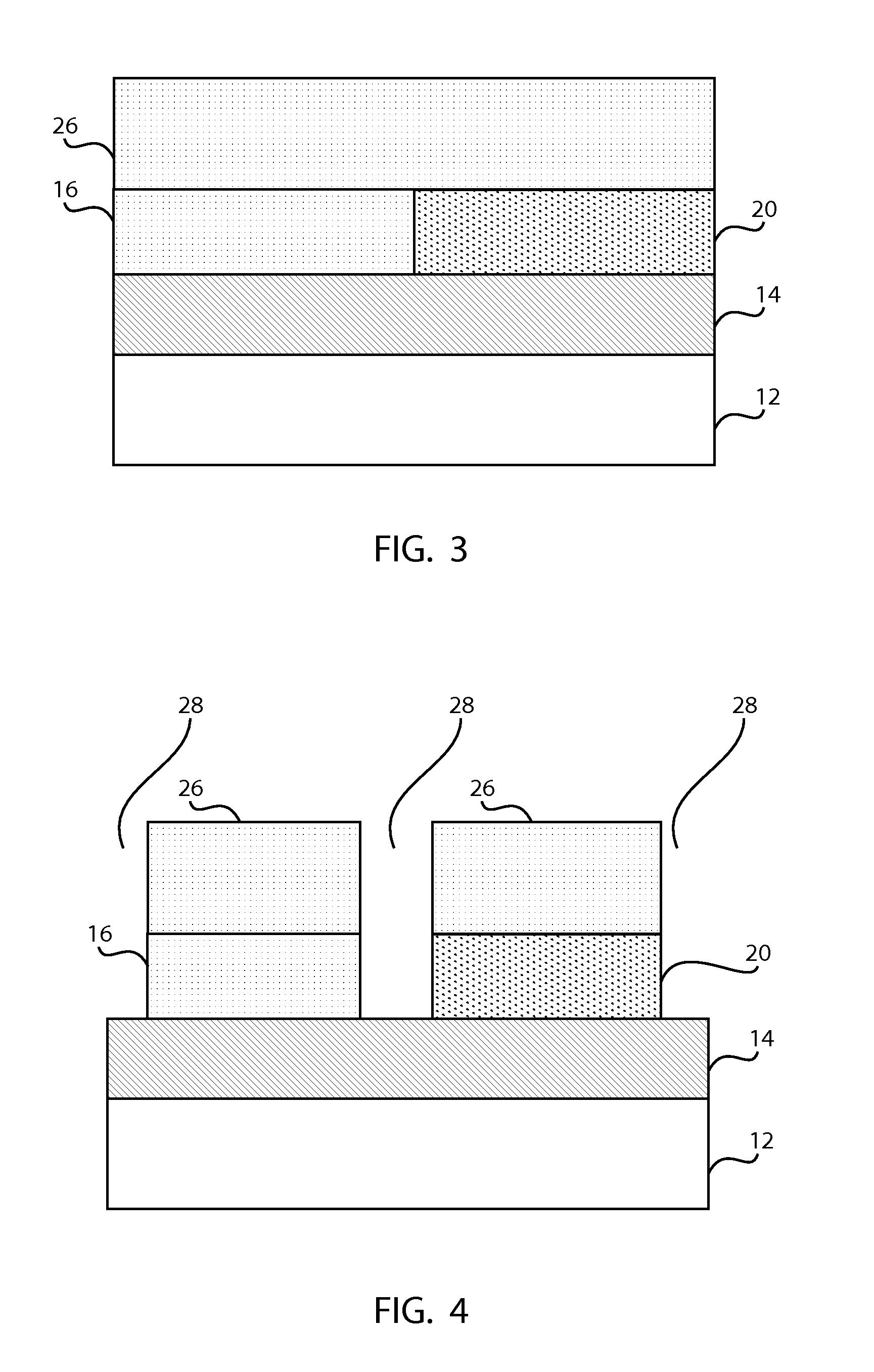
The patent text describes a method for making complementary metal oxide semiconductor devices by forming various layers on a silicon substrate. The method includes masking a portion of a silicon layer with a hard mask, doping another portion of the silicon layer, growing an undoped silicon layer, removing the hard mask, relaxing strain in the silicon layer, growing a SiGe layer, oxidizing the SiGe layer, etching fins in a first portion of the silicon layer and in a second portion of the silicon layer, and forming a converted dielectric layer on the substrate. The method can produce devices with different strain states in the silicon layers, which can enhance performance. The resulting device includes first fins in a first region and second fins in a second region on a silicon layer, with different heights. The first fins are in N-type field effect transistors, and the second fins are in P-type field effect transistors.

Problems solved by technology

However, forming a dually strained channel (tensile for NFET and compressive for PFET) is challenging.

Method used


Image

  • Porous silicon relaxation medium for dislocation free CMOS devices
  • Porous silicon relaxation medium for dislocation free CMOS devices
  • Porous silicon relaxation medium for dislocation free CMOS devices

Examples


Embodiment Construction

[0027]In accordance with the present principles, methods and structures are provided for forming tensile strained NFETs and compressive strained PFETs on a same chip. Both NFETs and PFETs have a dielectric layer formed under a channel to provide improved isolation that is better than junction isolation. In accordance with useful embodiments, a tensily strained silicon-on-insulator (sSOI) has a hard mask formed thereon to cover an NFET region while a PFET region is exposed. In one embodiment, boron is doped in the sSOI in the PFET region followed by epitaxially growing undoped Si on top of the boron-doped sSOI. NFET and PFET active regions are then patterned. The boron-doped sSOI is converted into porous Si so that the epitaxy Si relaxes. The porous Si is converted into an oxide to serve as an anchor for the relaxed Si. Then, SiGe is epitaxially grown on top of the relaxed Si to form compressively strained SiGe for the PFET. In this way, both tensile and compressive regions (for NFET...


PUM

PropertyMeasurementUnit
porosityaaaaaaaaaa
porosityaaaaaaaaaa
tensile-strainedaaaaaaaaaa

Abstract

A method for forming CMOS devices includes masking a first portion of a tensile-strained silicon layer of a SOI substrate, doping a second portion of the layer outside the first portion and growing an undoped silicon layer on the doped portion and the first portion. The undoped silicon layer becomes tensile-strained. Strain in the undoped silicon layer over the doped portion is relaxed by converting the doped portion to a porous silicon to form a relaxed silicon layer. The porous silicon is converted to an oxide. A SiGe layer is grown and oxidized to convert the relaxed silicon layer to a compressed SiGe layer. Fins are etched in the first portion from the tensile-strained silicon layer and the undoped silicon layer and in the second portion from the compressed SiGe layer.

Description

BACKGROUND[0001]Technical Field[0002]The present invention relates to semiconductor processing, and more particularly to devices and methods for fabricating complementary metal oxide semiconductor (CMOS) devices having compressive and tensile stressed channel materials.[0003]Description of the Related Art[0004]Strain engineering is highly desired for boosting CMOS performance. Tensile strain is beneficial for N-type field effect transistors (NFETs), and compressive strain is beneficial for P-type field effect transistors (PFETs). Conventional external strain techniques such as, embedded source / drain, stress liner, etc. begin to lose their effectiveness due to highly scaled pitches and the three-dimensional (3D) nature of fin field effect transistors (finFETs).[0005]Channel strain is one option that still works regardless of pitches and device architectures. However, forming a dually strained channel (tensile for NFET and compressive for PFET) is challenging.SUMMARY[0006]A method for...

Claims


Application Information

Patent Timeline
Patent Type & Authority Applications(United States)
IPC IPC(8): H01L27/12H01L21/84H01L21/8238H01L21/326H01L21/02H01L21/306H01L29/167H01L27/092H01L29/161
CPCH01L27/1211H01L21/845H01L21/76227H01L27/0924H01L27/0922H01L21/823821H01L21/823807H01L29/161H01L21/02532H01L21/02236H01L21/30604H01L29/167H01L21/326H01L21/26506H01L21/7624H01L29/0649H01L29/7849H01L29/785
Inventor CHENG, KANGGUODIVAKARUNI, RAMACHANDRAKIM, JEEHWANLI, JUNTAOSADANA, DEVENDRA K.
Owner ELPIS TECH INC
Learn More