Touch display device
- Summary
- Abstract
- Description
- Claims
- Application Information
AI Technical Summary
Benefits of technology
Problems solved by technology
Method used
Image
Examples
Embodiment Construction
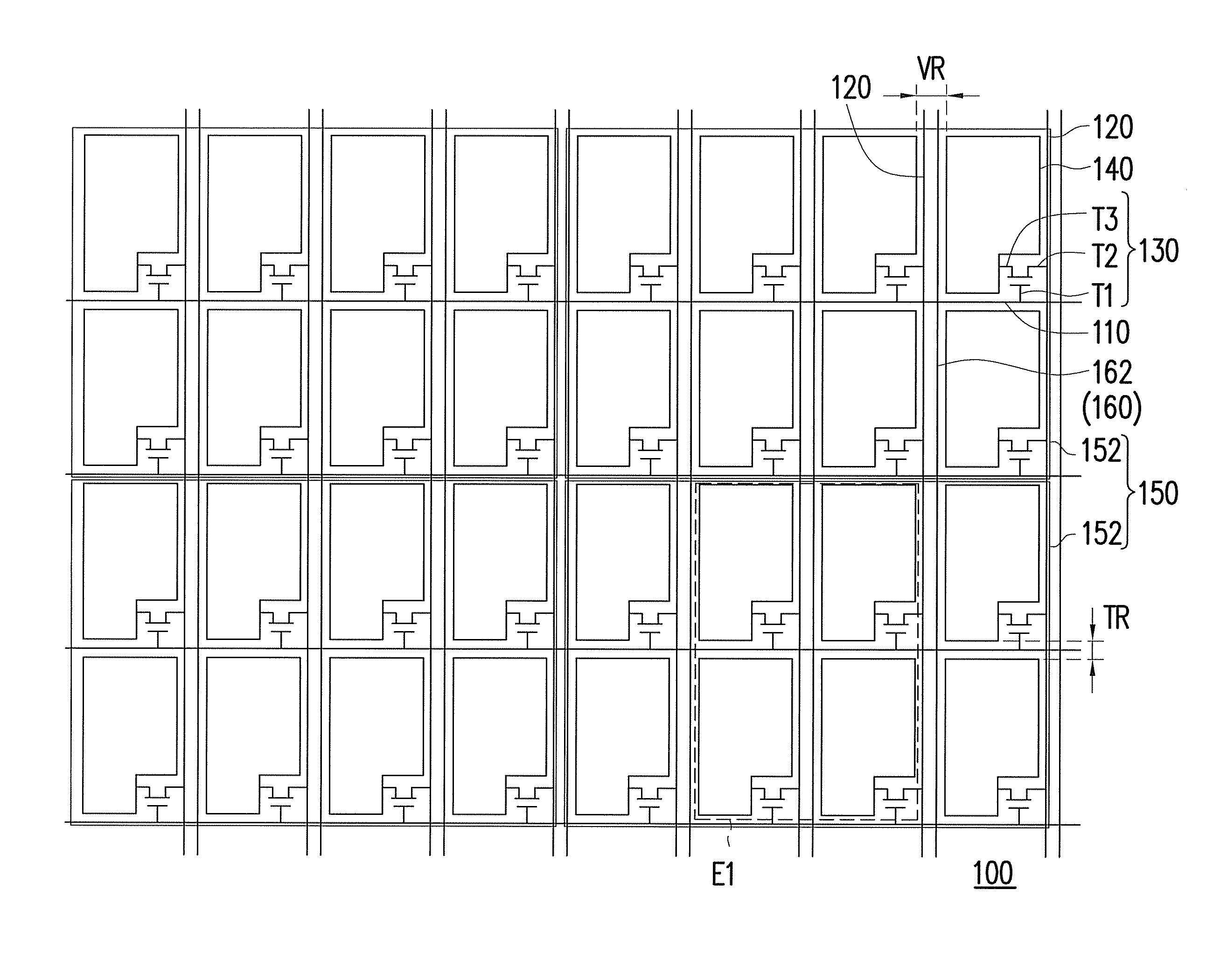
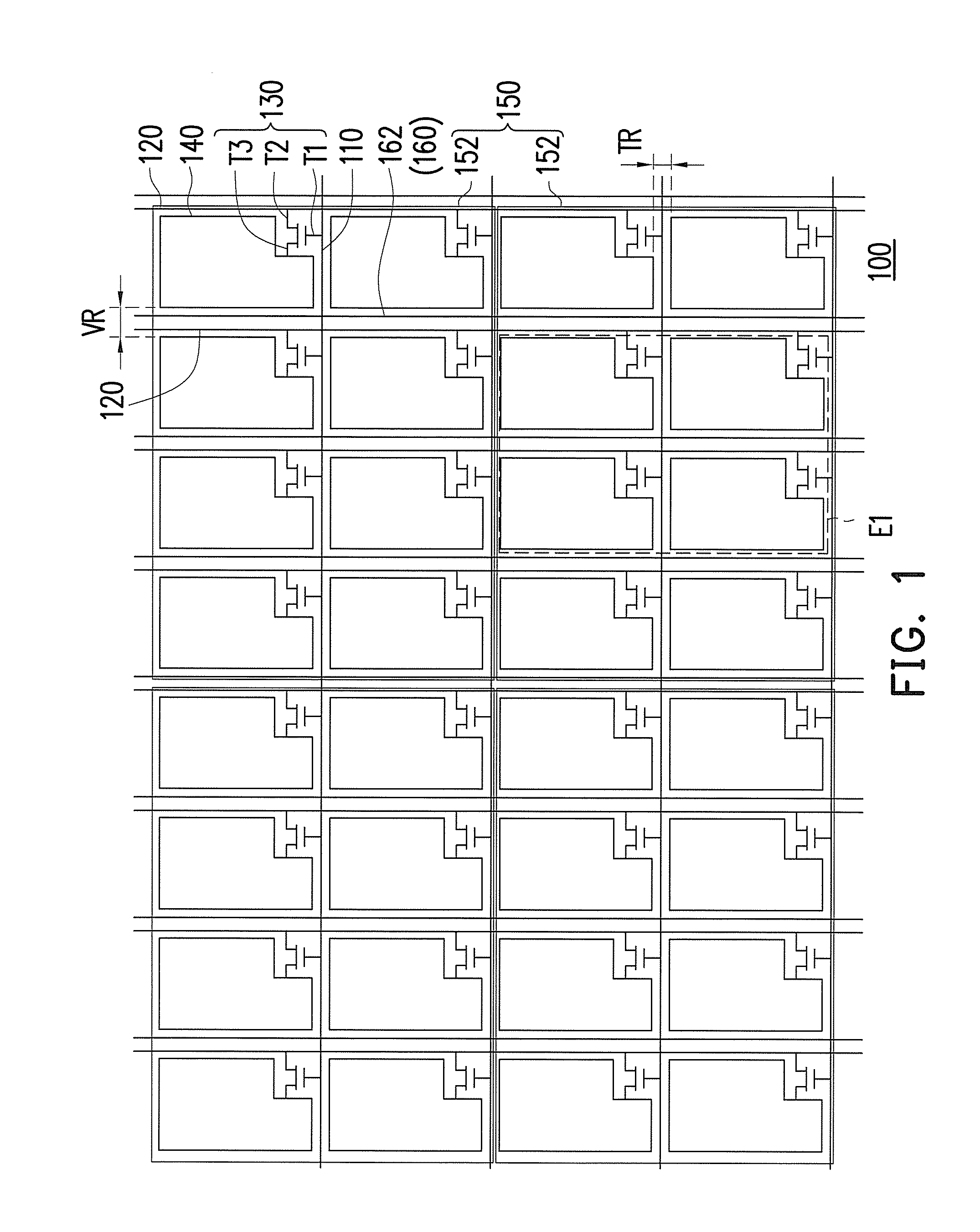
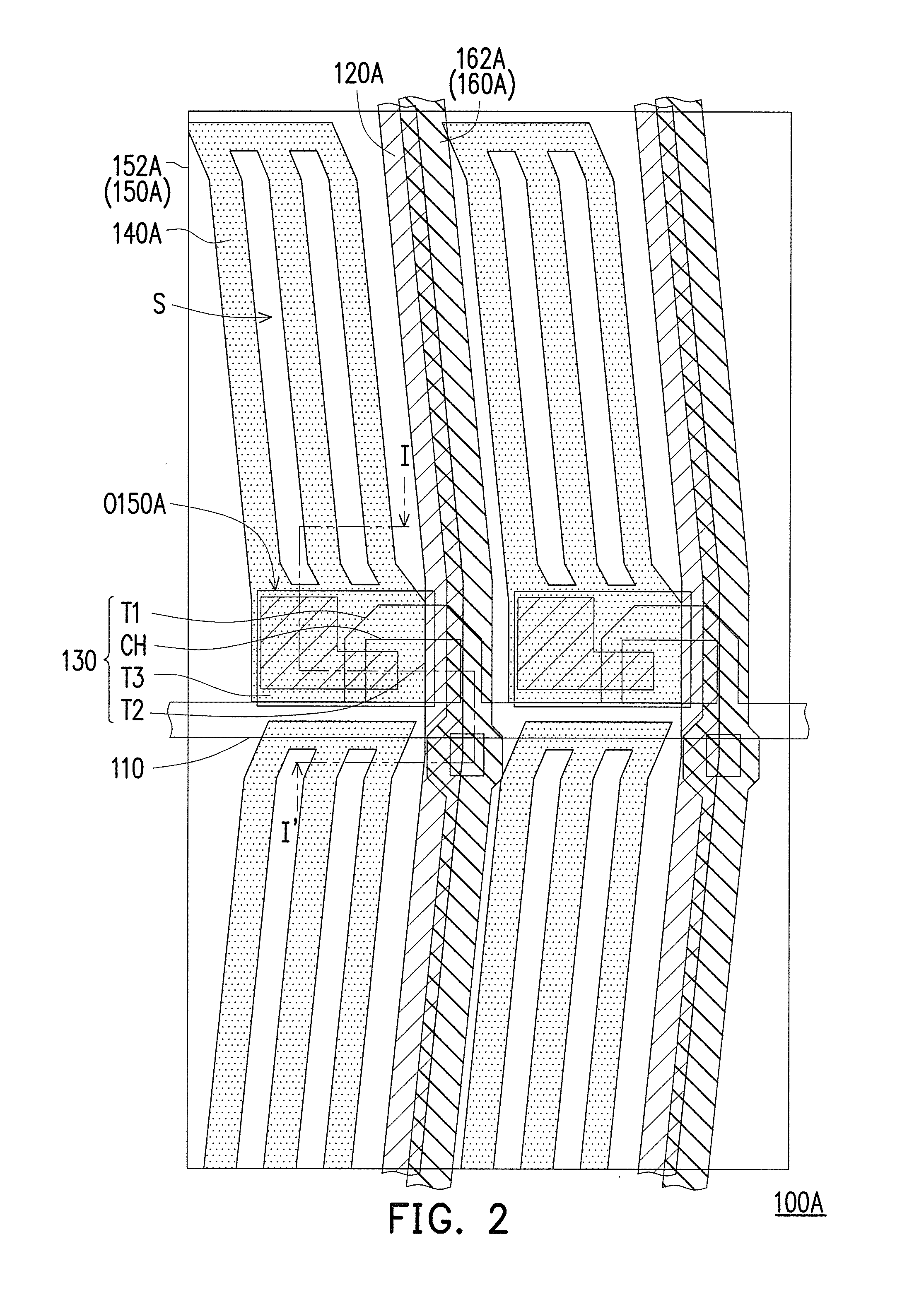
[0049]FIG. 1 is a schematic diagram illustrating a pixel array structure according to an embodiment of the invention. Referring to FIG. 1, a pixel array structure 100 includes a plurality of scan lines 110, a plurality of data lines 120, a plurality of active devices 130, a plurality of pixel electrodes 140, a signal electrode layer 150 and a signal transmission layer 160. The data lines 120 intersect the scan lines 110. The active devices 130 are connected with the scan lines 110 and the data lines 120. The pixel electrodes 140 are connected with the active devices 130. The pixel electrodes 140 are arranged in an array, and a vertical wiring area VR is located between the pixel electrodes 140 of each two adjacent columns. The signal electrode layer 150 and the pixel electrodes 140 are stacked in the thickness direction, and the signal electrode layer 150 includes a plurality of signal electrodes 152 which are separated from one another. The signal transmission layer 160 includes a ...
PUM
 Abstract
Description
Claims
Application Information
 - R&D
- Intellectual Property
- Life Sciences
- Materials
- Tech Scout
- Unparalleled Data Quality
- Higher Quality Content
- 60% Fewer Hallucinations
Browse by: Latest US Patents, China's latest patents, Technical Efficacy Thesaurus, Application Domain, Technology Topic, Popular Technical Reports.
© 2025 PatSnap. All rights reserved.Legal|Privacy policy|Modern Slavery Act Transparency Statement|Sitemap|About US| Contact US: help@patsnap.com


