Thin film transistor, method of manufacturing thin film transistor, array substrate and display device

a thin film transistor and array substrate technology, applied in the field can solve the problems of not being adapted to the current development of the display application, difficulty in achieving uniformity in this type of thin film transistor, and low mobility of carriers of amorphous silicon thin film transistors, so as to improve enhance the performance of thin film transistors

Inactive Publication Date: 2016-11-24
BOE TECH GRP CO LTD
View PDF5 Cites 11 Cited by
  • Summary
  • Abstract
  • Description
  • Claims
  • Application Information

AI Technical Summary

Benefits of technology

[0008]Therefore, embodiments of the present invention provide a thin film transistor, a method of manufacturing a thin film transistor, an array substrate and a display device, for avoiding damage on the active layer when etching a source-drain electrode layer.
[0030]Preferably, in the method of manufacturing the thin film transistor according to the embodiment of the present invention, the source-drain electrode is made of copper, which may render reduced resistance; and
[0042]The thin film transistor, the method of manufacturing a thin film transistor, the array substrate and the display device ensure electrical connection between the source and drain electrodes and the active layer without configuring any through hole due to providing the etch stop layer between the active layer and the source and drain electrodes, a portion of which being in contact with the source and drain electrodes is made of metal or metal alloy; and may ensure insulation between the source electrode and the drain electrode when the thin film transistor is turned-off, ensuring normal operation of the thin film transistor, by oxidating the portion of the etch stop layer at the position between the source electrode and the drain electrode as insulating material through the oxidation process. In the above thin film transistor, the etch stop layer may not only prevent the active layer from being damaged when etching the source-drain electrode layer, but also prevent the active layer from other adverse effects from subsequent processes, such as adverse effects from water, hydrogen and oxygen, etc., thereby enhancing performance of the thin film transistor, just because of providing the etch stop layer between the active layer and the source-drain electrode layer in the thin film transistor. The provision of the etch barrier layer may improve performance of the thin film transistor.

Problems solved by technology

However, an amorphous silicon thin film transistor has a rather low mobility of carriers, such as 0.1˜1 cm2V−1 s−1 of mobility of electron, and thus is not adapted to the current development of the display application.
However, there is still a difficulty in achieving uniformity in this type of thin film transistor.
Thus, when used in a large-size panel, it will be subjected to great impediment.
However, when etching the source-drain electrode layer, the oxide active layer may be damaged, which cannot be avoided even adjustment had been made on the etchant.
In this instance, the thin film transistor may be degraded in performance, even be damaged to have no properties of switch.

Method used


Image

  • Thin film transistor, method of manufacturing thin film transistor, array substrate and display device
  • Thin film transistor, method of manufacturing thin film transistor, array substrate and display device
  • Thin film transistor, method of manufacturing thin film transistor, array substrate and display device

Examples


Embodiment Construction

[0049]Embodiments of a thin film transistor, a method of manufacturing the thin film transistor, an array substrate and a display device according to embodiments of the present are described below in detail in combination with drawings.

[0050]In the drawings, thickness and shape of various films or layers do not reflect actual scale of the thin film transistor and the array substrate, but are intended to illustrate the scheme of the present disclosure.

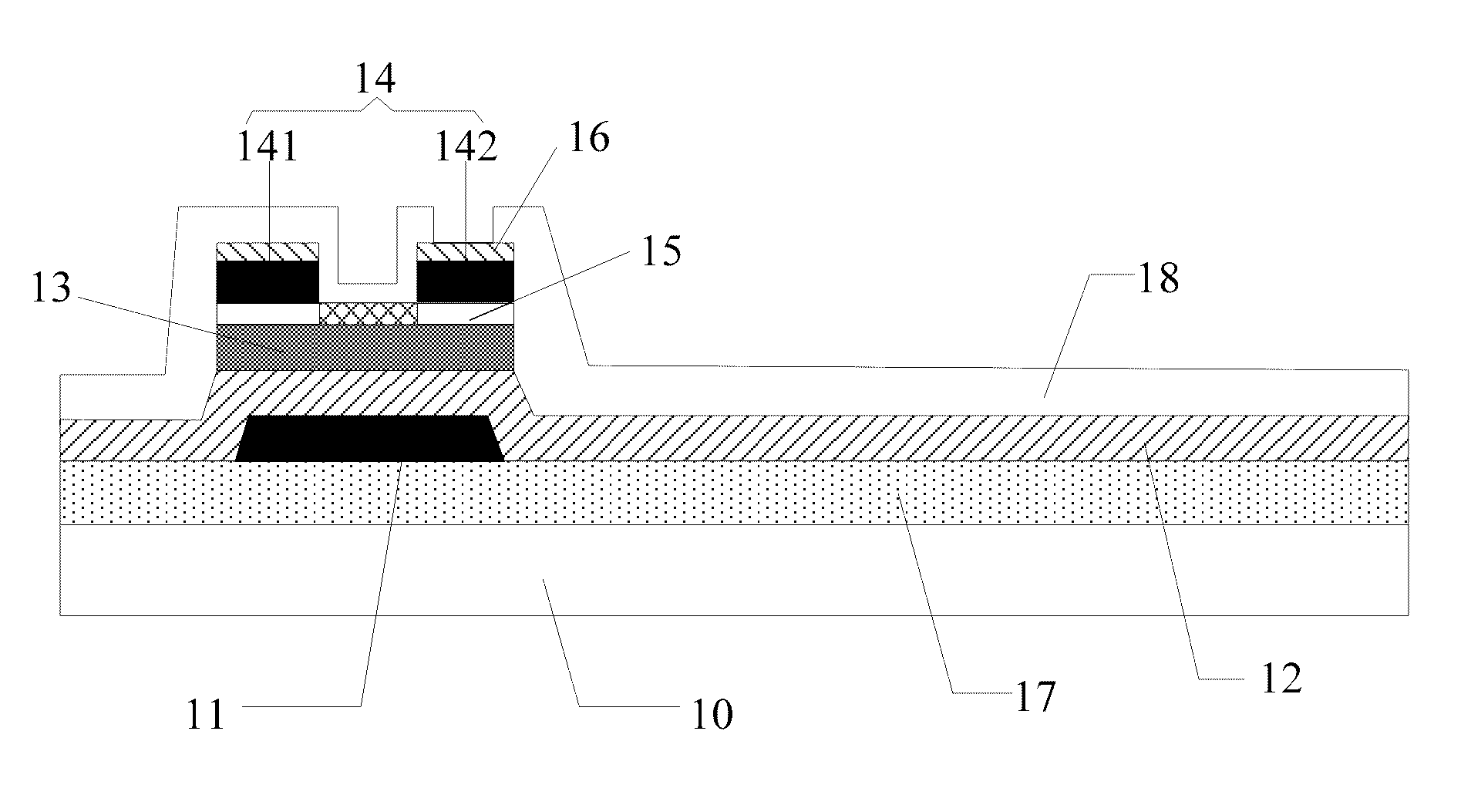
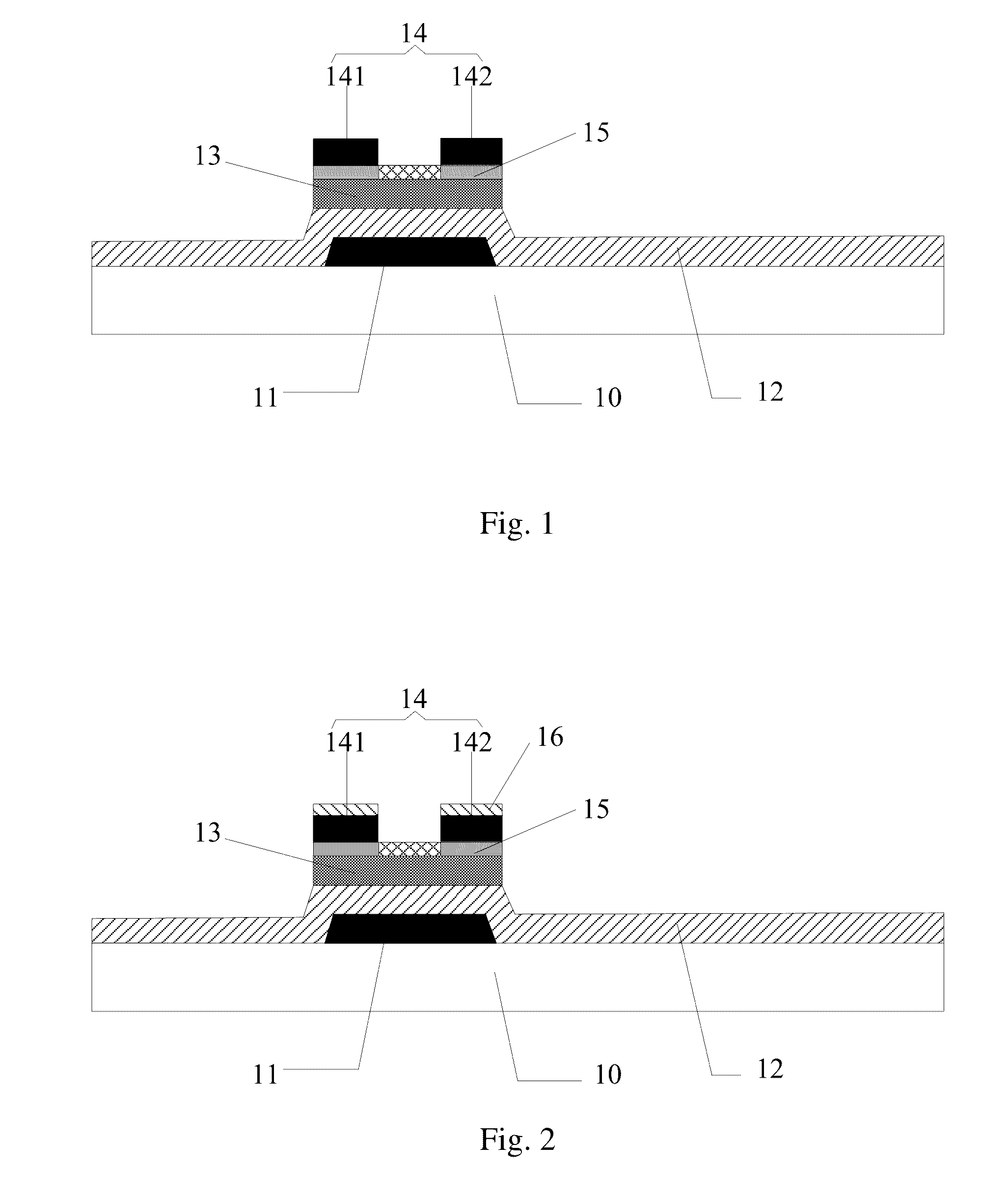
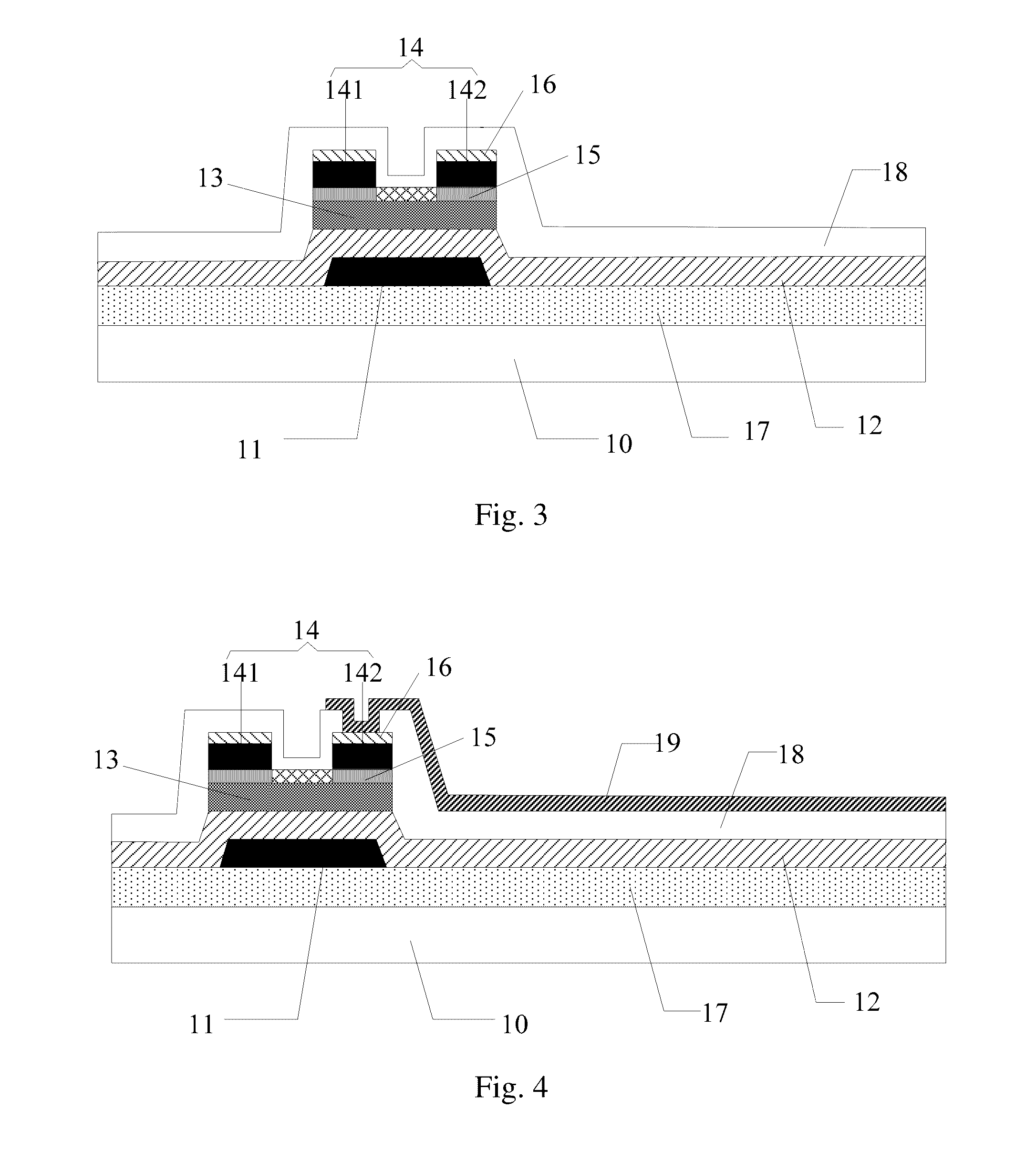
[0051]Embodiments of the present invention provide a thin film transistor, as shown in FIG. 1. The thin film transistor includes: a base substrate 10, and a gate electrode 11, a gate insulating layer 12, an active layer 13 and source-drain electrode layer 14, which are in turn located on the base substrate 10.

[0052]The thin film transistor further includes: an etch stop layer 15 located between the active layer 13 and the source-drain electrode layer 14, wherein orthogonal projection of the etch stop layer 15 on the base substrate 10 is...


PUM


Abstract

Embodiments of the present invention disclose a thin film transistor, a method of manufacturing a thin film transistor, an array substrate and a display device, which may ensure electrical connection between source and drain electrodes and an active layer without configuring any through hole due to providing an etch stop layer between the active layer and the source and drain electrodes, a portion of the etch stop layer being in contact with the source and drain electrode is made of metal or metal alloy; and may ensure insulation between the source and the drain electrodes when the thin film transistor is turned-off, ensuring normal operation of the thin film transistor, by oxidating the portion of the etch stop layer at the position between the source and the drain electrodes as an insulating material. The etch stop layer may not only prevent the active layer from being damaged when etching the source and drain electrodes, but also prevent the active layer from other adverse effects from subsequent processes, such as adverse effects from water, hydrogen and oxygen, etc., thereby enhancing performance of the thin film transistor, just because of providing the etch stop layer between the active layer and the source and drain electrodes in the thin film transistor.

Description

CROSS-REFERENCE TO RELATED APPLICATIONS[0001]This application claims priority of Chinese Application No. 201510254665.X, filed May 18, 2015, entitled “Thin film transistor, method of manufacturing a thin film transistor, array substrate and display device”, which is incorporated herein by reference in their entirety.BACKGROUND[0002]1. Technical Field[0003]The present invention relates to field of semiconductor technology, and particularly to a thin film transistor, a method of manufacturing a thin film transistor, an array substrate and a display device.[0004]2. Description of the Related Art[0005]As application of a flat panel display is developing, requirements on a display panel become higher. Particularly, mobility of a thin film transistor in the display panel is needed to be in higher level. Recently, an existing thin film transistor is often an amorphous silicon thin film transistor, i.e., an active layer of the thin film transistor is made of amorphous silicon material. Howe...

Claims


Application Information

Patent Timeline
Patent Type & Authority Applications(United States)
IPC IPC(8): H01L27/12H01L33/42H01L29/66H01L29/45H01L29/786
CPCH01L27/1225H01L29/458H01L33/42H01L29/66969H01L27/124H01L29/7869H01L29/45
Inventor LIU, XIANG
Owner BOE TECH GRP CO LTD
Why Eureka
Try Eureka