Nanoparticle material and light-emitting device

a technology of nanoparticles and light-emitting devices, which is applied in the direction of chemistry apparatus and processes, metal selenides/tellurides, and luminescent compositions. it can solve the problems of poor recombination probability of carriers, poor performance of confining carriers, poor performance of confining carriers, etc., and achieve excellent hole block function, improve the tunneling transport properties of carriers, and low drive voltage

Active Publication Date: 2016-08-04
MURATA MFG CO LTD
View PDF10 Cites 17 Cited by
  • Summary
  • Abstract
  • Description
  • Claims
  • Application Information

AI Technical Summary

Benefits of technology

[0056]This combination of the first quantum dot with the second quantum dot that has the thin shell part of less than 3 ML in thickness improves the tunneling transport properties of carriers, thereby making it possible to realize a high-efficiency light-emitting device which has a low drive voltage and an excellent hole block function.
[0057]The nanoparticle material according to the present invention has the core-shell structure including the core part and the shell part coating the core part, and the shell part has a thickness of 3 to 5 ML on the basis of the constituent molecule of the shell part, and thus has an adequate thickness. Thus, even when the nanoparticle material is used for a light-emitting layer of a light-emitting device, the hole blocking performance can be improved while a decrease in carrier transport properties is avoided as much as possible, without generation of any surface defect due to lattice mismatch between the nanoparticle material and the core material.
[0058]In addition, the ...

Problems solved by technology

However, in Patent Document 1 (FIG. 18), while crystals have few surface defects because the InGaAs constituting the quantum dots 103 is formed by epitaxial growth, the InGaAs has some of In substituted with Ga, and therefore makes a small difference in bandgap energy between the InGaAs and the GaAs that forms the substrate 101 and the coating layer 102, and has poor performance of confining carriers.
However, in the Patent Document 1, since the difference in bandgap energy is small between the InGaAs that forms the quantum dots 103 and the GaAs that forms the substrate 101 and the coating layer 102, there is a possibility that without recombination of holes transported from a hole transpor...

Method used


Image

  • Nanoparticle material and light-emitting device
  • Nanoparticle material and light-emitting device
  • Nanoparticle material and light-emitting device

Examples


first embodiment

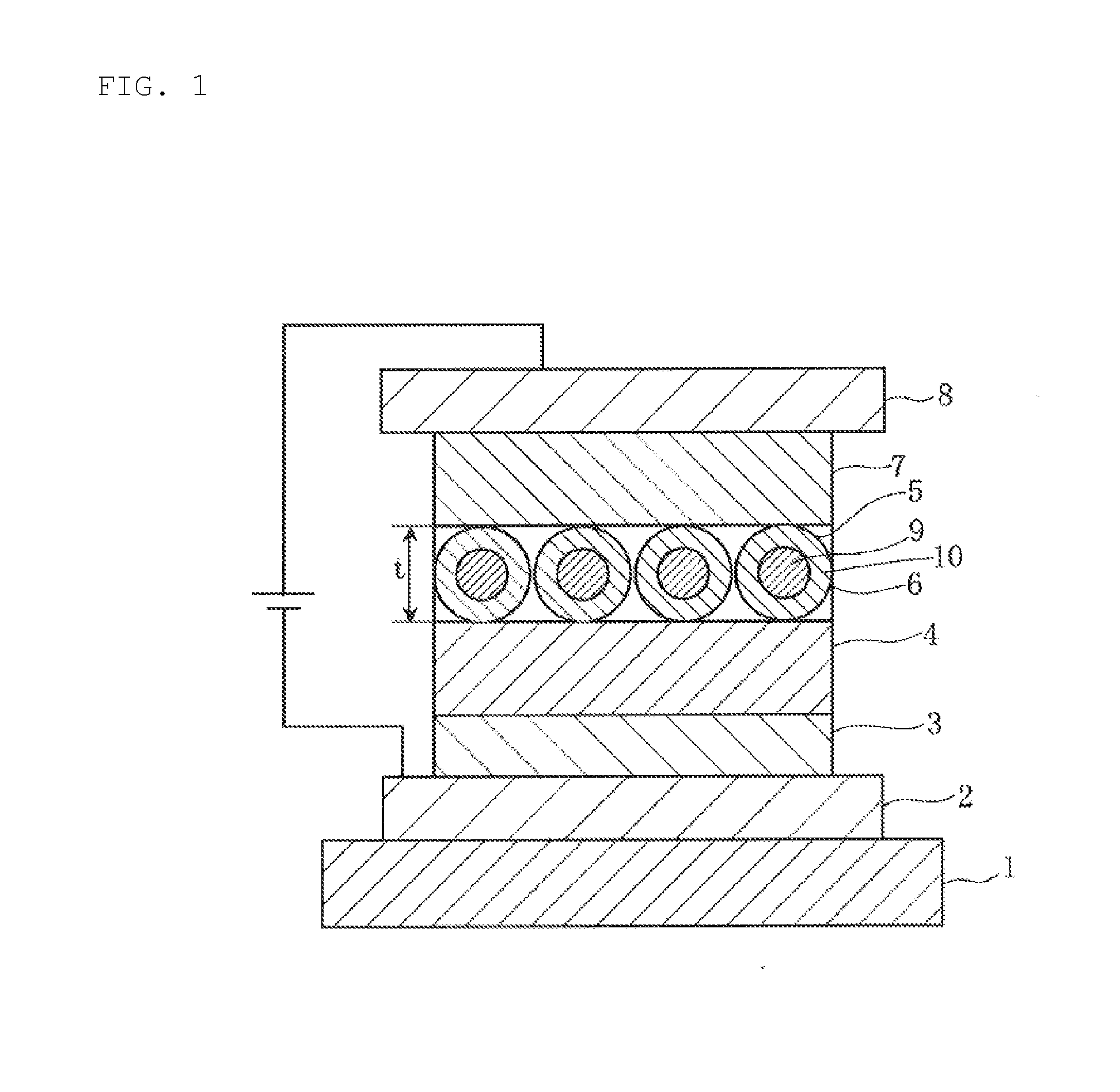
[0082]FIG. 1 is a cross-sectional view schematically illustrating a first embodiment of an EL element as a light-emitting device according to the present invention, where a light-emitting layer is formed from a nanoparticle material according to the present invention.

[0083]That is, this EL element has an anode 2 formed on a transparent substrate 1 such as a glass substrate, a hole injection layer 3 and a hole transport layer 4 composed of hole transporting materials sequentially formed on the surface of the anode 2, and a light-emitting layer 6 with a thickness t formed on the surface of the hole transport layer 4. In addition, an electron transport layer 7 composed of an electron transporting material is formed on the surface of the light-emitting layer 6, and a cathode 8 is formed on the surface of the electron transport layer 7.

[0084]Then, in the light-emitting layer 6, quantum dots 5 that is a nanoparticle material according to the present invention are aligned in a matrix.

[0085...

second embodiment

[0140]FIG. 6 is a cross-sectional view schematically illustrating a second embodiment of an EL element as a light-emitting device according to the present invention.

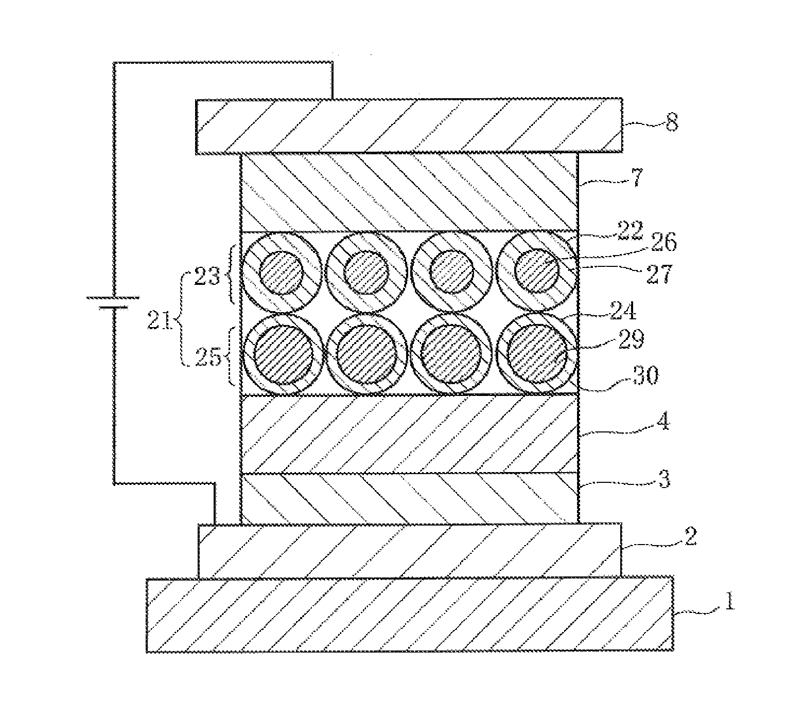
[0141]This EL element has a stacked structure where a light-emitting layer 21 has a first light-emitting layer 23 formed from first quantum dots 22 and a second light-emitting layer 25 formed from second quantum dots 24 that are smaller in shell part thickness than the first quantum dots 22.

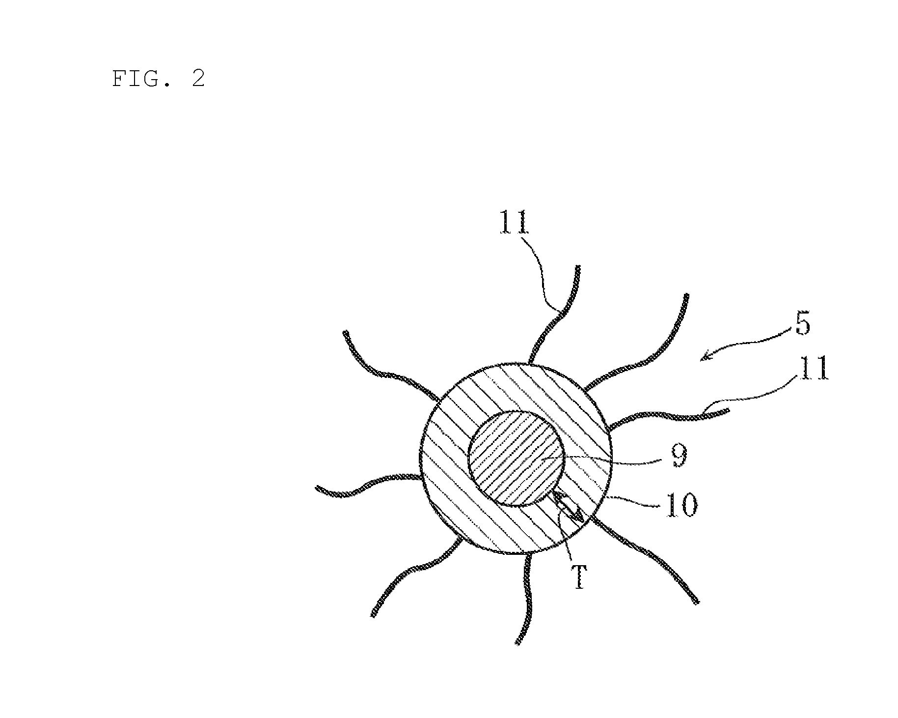
[0142]The first quantum dot 22 has, specifically as illustrated in FIG. 7, the same form as in the first embodiment, and a shell part 27 is formed on the surface of a core part 26, while the surface of the shell part 27 is coated with a surfactant 28, and the thickness T of the shell part 27 is 3 to 5 ML on the basis of the constituent molecule of the shell part 27.

[0143]In addition, the second quantum dot 24 has, as illustrated in FIG. 8, a core-shell structure composed of a core part 29 and a shell part 30 coating the core part 29, ...

example 1

Preparation of Sample

[0163](Sample Number 1)

[0164](Preparation of Quantum Dot Dispersing Solution)

[0165]A quantum dot dispersing solution composed of a core part of CdSe (LUMO level: 4.4 eV, HOMO level: 6.5 eV) and a shell part of ZnS (LUMO level: 3.9 eV, HOMO level: 7.4 eV) was prepared.

[0166]That is, a cadmium oxide and a stearic acid were weighed to provide the cadmium oxide: 1.6 mmol and the stearic acid: 6.4 mmol. Then, the cadmium oxide and the stearic acid were put into a round-bottom flask with octadecene: 16 mL retained therein, and mixed in the octadecene. Then, this mixture was stirred with a stirring bar for 30 minutes while being heated to 100° C. under reduced pressure, further stirred with a stirring bar for 1 hour while being heated to 200° C. under a nitrogen atmosphere, and cooled to room temperature. Thereafter, to this solution, TOPO: 4 g and octadecylamine: 12 g were added, and the solution was again stirred with a stirring bar for 30 minutes while being heated ...


PUM


Abstract

Quantum dots (nanoparticle material) each having a core-shell structure including a core part and a shell part that protects the core part. The shell part of the quantum dot has a thickness T of 3 to 5 ML based on the constituent molecule of the shell part. A light-emitting device includes the quantum dots.

Description

CROSS REFERENCE TO RELATED APPLICATIONS[0001]The present application is a continuation of International application No. PCT / JP2014 / 077585, filed Oct. 16, 2014, which claims priority to Japanese Patent Application No. 2013-216634, filed Oct. 17, 2013, the entire contents of each of which are incorporated herein by reference.FIELD OF THE INVENTION[0002]The present invention relates to a nanoparticle material and a light-emitting device, more specifically, to a nanoparticle material that has a core-shell structure, and a light-emitting device such as an EL element (EL: Electro Luminescence) with a light-emitting layer formed with the use of the nanoparticle material.BACKGROUND OF THE INVENTION[0003]Quantum dots that are nanoparticles of 10 nm or less in particle size have excellent performance of confining carriers (electrons, holes), and can thus easily produce excitons by recombination of electrons and holes. For this reason, luminescence from free excitons can be expected, and it is...

Claims


Application Information

Patent Timeline
IPC IPC(8): H01L33/06C09K11/88
CPCB82Y20/00B82Y30/00C01B19/007C01P2004/04C01P2004/64C01P2004/80H01L33/06C09K11/883H05B33/14H01L31/028H01L31/0296H01L31/0304H01L31/035218C09K11/565H10K50/11H10K2101/40H10K50/115H10K50/13H10K2102/351
Inventor MURAYAMA, KOJIMIYATA, HARUYA
Owner MURATA MFG CO LTD
Why Eureka
Try Eureka