
Method of Fabricating an Electronic Device

a technology of electronic components and manufacturing methods, applied in the direction of semiconductor devices, semiconductor/solid-state device details, electrical apparatus, etc., can solve the problems of affecting the performance of electronic components, generating heat in the operation of electronic components, and negatively affecting the mean time between failures

Inactive Publication Date: 2016-07-07
DOW CORNING CORP
View PDF3 Cites 16 Cited by
  • Summary
  • Abstract
  • Description
  • Claims
  • Application Information

AI Technical Summary

Benefits of technology

This patent text discusses the issue of poor heat transfer in electronic components and how using a thermally conductive material (TIM) can improve it. However, the surfaces of the components may not be perfectly smooth, creating air spaces that impair heat transfer. To address this, applied pressure can improve the thermal resistance of the TIM, allowing for better heat transfer. This pressure can be applied during the curing process or throughout the device's use. Overall, this patent provides a solution for improving heat transfer in electronic components.

Problems solved by technology

However, the operation of an electronic component generates heat.
Excessive temperatures can adversely affect performance of the electronic component and operation of the electronic device associated therewith and negatively impact mean time between failures.
Surfaces of the electronic component and the IHS or heat sink may not be completely smooth, and therefore, it is difficult to achieve full contact between the surfaces.
Air spaces, which are poor thermal conductors, appear between the surfaces and impede the removal of heat.
However, such multi-chip packages place additional requirements on the thermal management solutions.
However, since it is not in the multi-chip package's center, warpage can be generated as a result of mismatches in coefficients of thermal expansion (CTE) of different components in the multi-chip package.
This CTE mismatch can place additional stress on the TIMs in the multi-chip package.

Method used

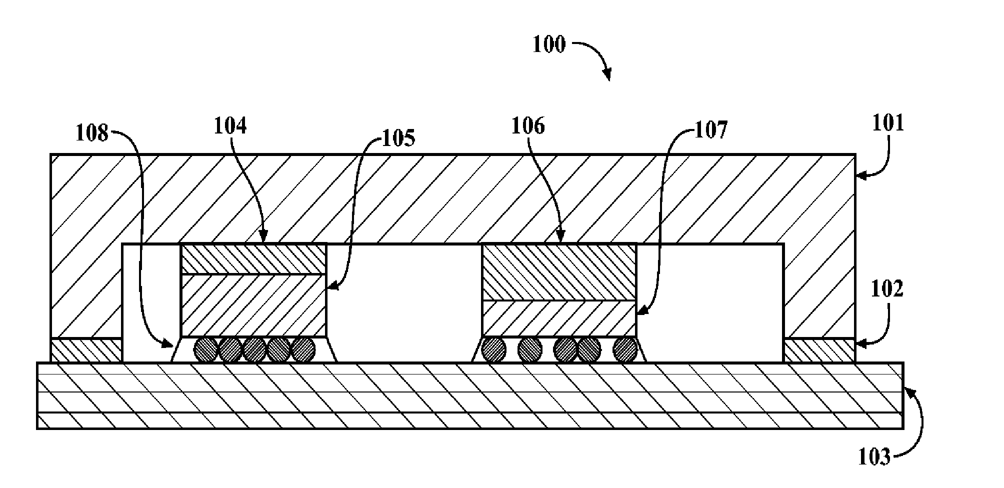
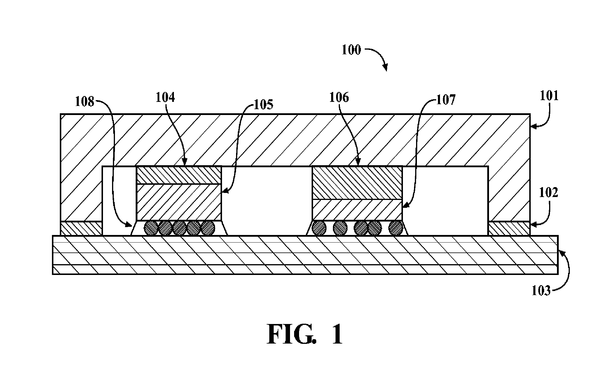

Image

  • Method of Fabricating an Electronic Device
  • Method of Fabricating an Electronic Device
  • Method of Fabricating an Electronic Device

Examples


examples

[0121]In these examples, “8-0080” refers to DOW CORNING® 8-0080, which is a mixture of vinyl-terminated polydimethylsiloxane and vinyl functional siloxane resin commercially available from Dow Corning Corporation of Midland, Mich., U.S.A. “Min-U-Sil®” refers to 5 um silica, “Cab-O-Sil® M-7D” refers to fumed silica, and “TS-530” refers to Cab-O-Sil® TS-530 fumed silica, all of which are commercially available from Cabot Corporation of Boston, Mass., U.S.A. “W-1011” refers to a carbon black pigment, which is commercially available from SID RICHARDSON CARBON COMPANY. “2-0707” refers to DOW CORNING® 2-0707, which is a platinum catalyst commercially available from Dow Corning Corporation. “6-3570” refers to DOW CORNING® 6-3570, which is a trimethylsiloxy-terminated poly(dimethyl,methylhydrogen siloxane) commercially available from Dow Corning Corporation. “PJ Fluid” refers to DOW CORNING® 4-2783, which is a hydroxy-terminated poly(methylvinylsiloxane) commercially available from Dow Corn...


PUM

PropertyMeasurementUnit
Fractionaaaaaaaaaa
Fractionaaaaaaaaaa
Thicknessaaaaaaaaaa

Abstract

A silicone composition contains I) a shrink additive and II) a curable polyorganosiloxane composition. A method for fabricating an electronic device includes the steps of: 1) interposing the silicone composition between an IHS and a substrate, 2) curing the curable polyorganosiloxane composition to form a cured silicone product, and 3) removing the shrink additive during and / or after step 2), thereby compressing the IHS to the substrate. Compressing occurs as thickness of the cured silicone product decreases, as compared to thickness of the silicone composition interposed in step 1).

Description

[0001]Electronic components such as semiconductors, transistors, integrated circuits (ICs), discrete devices, central processing units (CPUs), memory caches, and others known in the art are designed to operate at a normal operating temperature or within a normal operating temperature range. However, the operation of an electronic component generates heat. If sufficient heat is not removed, the electronic component will operate at a temperature significantly above its normal operating temperature. Excessive temperatures can adversely affect performance of the electronic component and operation of the electronic device associated therewith and negatively impact mean time between failures.[0002]To avoid these problems, heat can be removed by thermal conduction from the electronic component to a heat sink. The heat sink can then be cooled by any convenient means such as convection or radiation techniques. During thermal conduction, heat can be transferred from the electronic component t...

Claims


Application Information

Patent Timeline
IPC IPC(8): H01L23/367H01L21/48
CPCH01L21/4882H01L23/3675C08G77/12C08G77/20C09J183/04H01L23/10H01L23/3737H01L23/42H01L23/296H01L2224/32245
Inventor BHAGWAGAR, DORAB EDULLARSON, LYNDONSTEINBRECHER, KRISTENTONGE, JAMES
Owner DOW CORNING CORP
Learn More