
Ultra high resolution flat panel display having in-cell type touch sensor

a high-resolution, flat-panel display technology, applied in the field of ultra-high-resolution flat-panel display having an in-cell type touch sensor, can solve the problems of high parasitic capacitance between the gate line and the date line included into the display, the amount of mutual capacitance generated at sensing the touch is low, and the display has a much longer life time and endurance. , to achieve the effect of high density display, reduced parasitic capacitance between the touch electrode and the routing lin

Active Publication Date: 2016-06-30
LG DISPLAY CO LTD
View PDF14 Cites 15 Cited by
  • Summary
  • Abstract
  • Description
  • Claims
  • Application Information

AI Technical Summary

Benefits of technology

The present invention provides a display with a touch sensor that eliminates parasitic capacitance between the touch electrode and the routing line, while maintaining sufficient storage capacitance between the pixel electrode and the common electrode. This improves accuracy sensing performance in the ultra high density display. By thinning the insulating layer between the common electrode and the pixel electrode, a large amount of storage capacitance can be provided, and the area of contact holes for connecting the touch electrode and the routing line can be minimized. This reduces manufacturing costs and reduces manufacturing tact time.

Problems solved by technology

Further, sometimes the users have to learn how to use these input devices.
Therefore, the in-cell type can be much thinner than other types of touch sensitive displays and has a much longer life time and endurance.
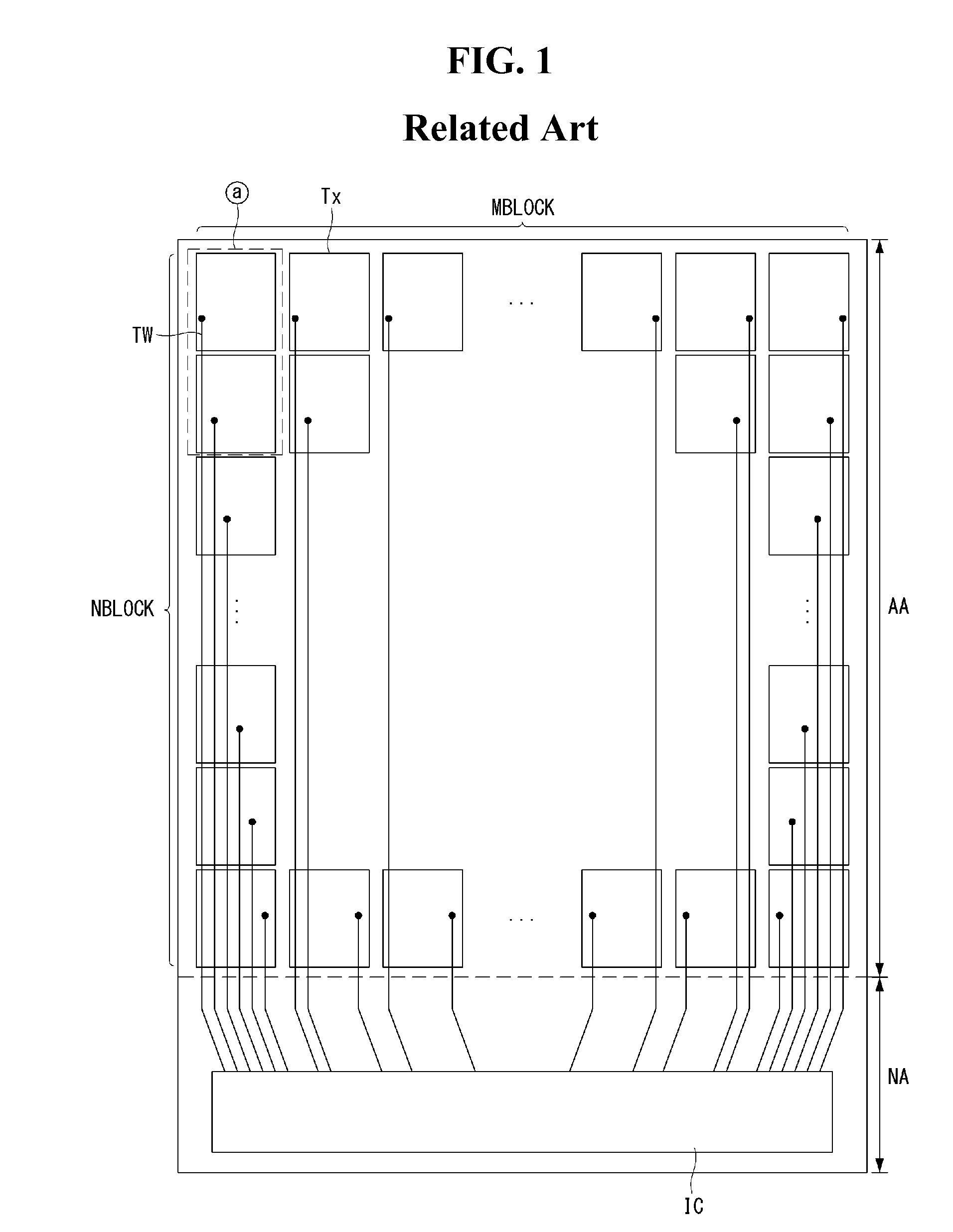
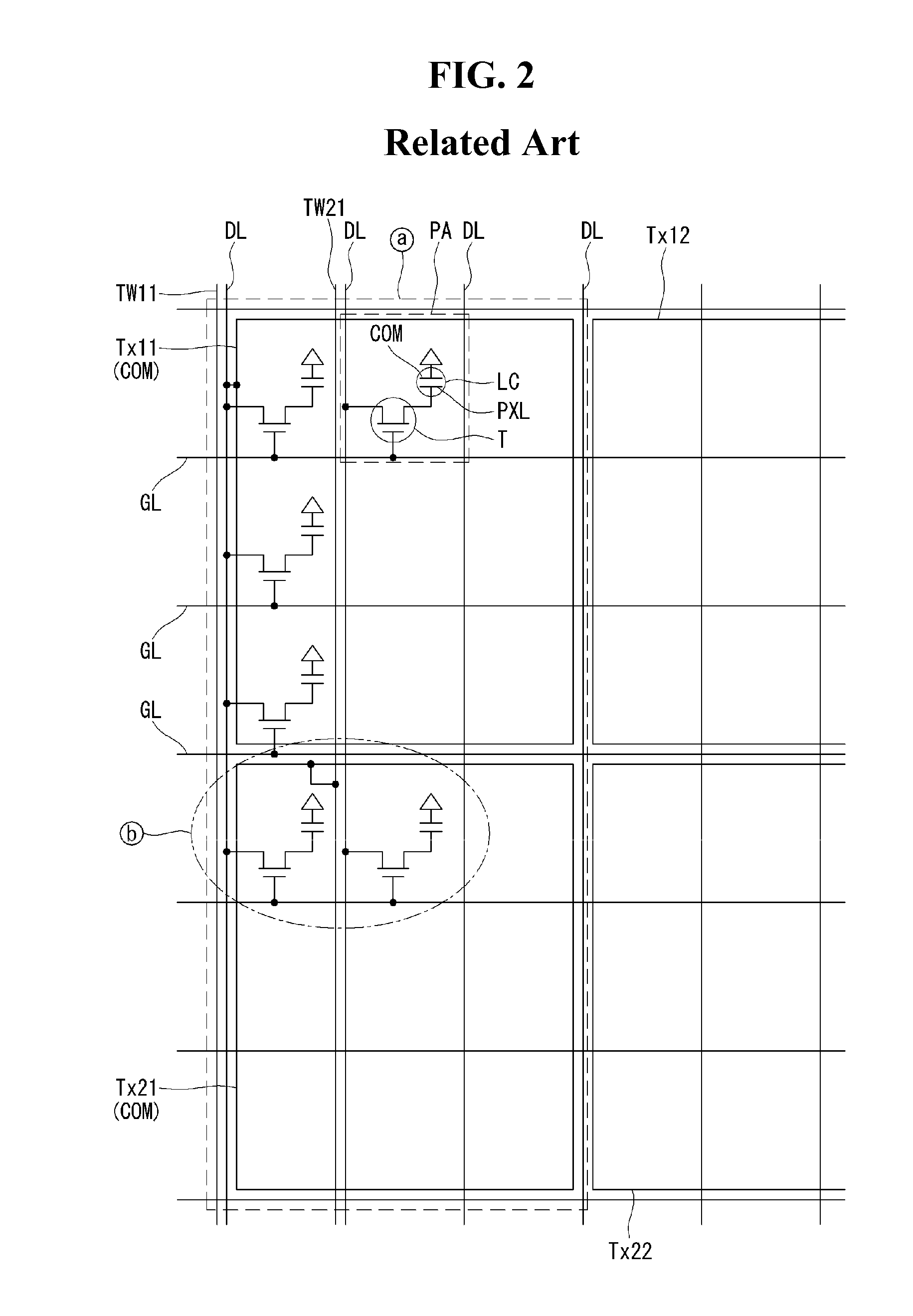
However, for the mutual capacitance type touch sensor, the amount of the mutual capacitance generated at sensing the touch is low, but the parasitic capacitances between the gate line and the date line included into the display are high.
Therefore, it may be hard to exactly decide where the touch action is detected, due to the interference of the parasitic capacitance.
Therefore, the line structure would be very complicated.
As the result, the high speed touch sensing is not possible.
However, in the ultra high density structure, the area of the pixel area PA is smaller and the elements are closer, so that it is very hard to ensure the area of the contact hole for good contact.

Method used


Image

  • Ultra high resolution flat panel display having in-cell type touch sensor
  • Ultra high resolution flat panel display having in-cell type touch sensor
  • Ultra high resolution flat panel display having in-cell type touch sensor

Examples


first embodiment

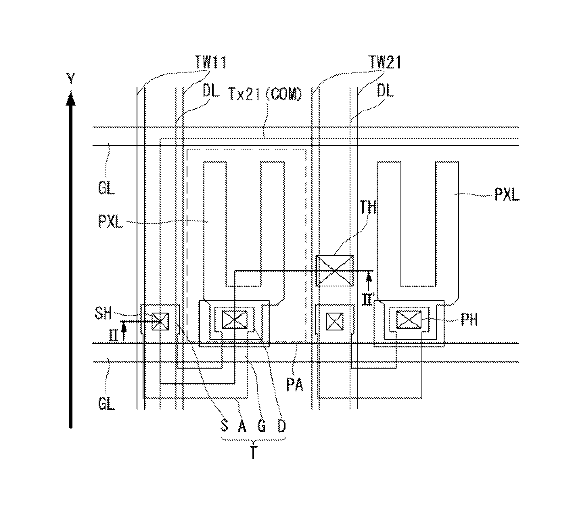
[0061]FIGS. 5 and 6 illustrate features of the first embodiment of the present disclosure. FIG. 5 is a plan view illustrating a structure of a liquid crystal display having a self capacitance touch sensor according to the first embodiment of the present disclosure. FIG. 6 is a cross section view, along the cutting line II-IF of FIG. 5, illustrating the structure of the liquid crystal display having the self capacitance touch sensor according to the first embodiment of the present disclosure.

[0062]Referring to FIGS. 5 and 6, a liquid crystal display having a self capacitance touch sensor according to the first embodiment of the present disclosure has a plurality of pixel areas PA disposed in a matrix manner defined by the crossing structure of a plurality of gate lines GL and a plurality of data lines DL on a substrate SUB. In each pixel area PA, a thin film transistor T, a pixel electrode PXL connected to the thin film transistor T and a common electrode COM facing with the pixel el...

second embodiment

[0074]FIGS. 7 and 8 illustrate the second embodiment of the present disclosure. FIG. 7 is a plan view illustrating a structure of a liquid crystal display having a self capacitance touch sensor according to the second embodiment of the present disclosure. FIG. 8 is a cross section view, along the cutting line III-III′ of FIG. 7, illustrating the structure of the liquid crystal display having the self capacitance touch sensor according to the second embodiment of the present disclosure.

[0075]Referring to FIGS. 7 and 8, a liquid crystal display embedding a self capacitance touch sensor according to the second embodiment of the present disclosure has a plurality of pixel areas PA disposed in a matrix manners defined by the crossing structure of a plurality of gate lines GL and a plurality of data lines DL on a substrate SUB. In each pixel area PA, a thin film transistor T, a pixel electrode PXL connected to the thin film transistor T and a common electrode COM facing with the pixel ele...


PUM


Abstract

A display having a touch sensor comprises: a plurality of pixel areas disposed in a matrix manner on a substrate; a routing line running along a first direction on the substrate; a first passivation layer covering the routing line; a touch electrode covering the routing line and corresponding to a grouped pixel areas on the first passivation layer; a touch contact hole exposing some portions of the routing line by penetrating the touch electrode and the first passivation layer; a second passivation layer covering the touch electrode; a passivation contact hole exposing the touch contact hole and some portions of the touch electrode around the touch contact hole by penetrating the second passivation layer; and a touch terminal connecting the touch electrode and the routing line on the second passivation layer.

Description

CROSS-REFERENCE TO RELATED APPLICATIONS[0001]This application claims the benefit of Korea Patent Application No. 10-2014-0194431 filed on Dec. 30, 2014, which is incorporated herein by reference for all purposes as if fully set forth herein.BACKGROUND[0002]1. Technical Field[0003]The present disclosure relates to an ultra high resolution flat panel display having an in-cell type touch sensor. Specifically, the present disclosure relates to an ultra high resolution flat panel display having the in-cell type touch sensor in which the parasitic capacitance between the touch electrode and the routing line is reduced and the storage capacitance between the common electrode and the pixel electrode can be ensured enough.[0004]2. Discussion of the Related Art[0005]Recently, as increasing the needs for display representing the various multimedia data, the flat panel displays are developed in large area with low price and high quality (high video quality, ultra high resolution, increased brig...

Claims


Application Information

Patent Timeline
IPC IPC(8): G06F3/041G09G3/36G09G3/20G06F3/044
CPCG06F3/0412G06F3/0416G09G3/2096G09G3/3648G06F3/044G06F3/0418G06F2203/04111G02F1/13338G06F3/04164G06F3/04166G06F3/0446G02F1/134372G02F1/1362
Inventor CHO, SEONGJUNKIM, KAKYUNGCHUNG, EUIHYUN
Owner LG DISPLAY CO LTD
Learn More