Semiconductor device and display apparatus
a technology of semiconductor devices and display devices, applied in the direction of semiconductor devices, electrical devices, transistors, etc., can solve the problems of rushing the development of thin-film transistors (tfts), which have excellent characteristics, and the drive circuit of active-matrix display apparatuses, and achieve the effect of reducing the parasitic capacitance between the gate line and the source lin
- Summary
- Abstract
- Description
- Claims
- Application Information
AI Technical Summary
Benefits of technology
Problems solved by technology
Method used
Image
Examples
embodiment 1
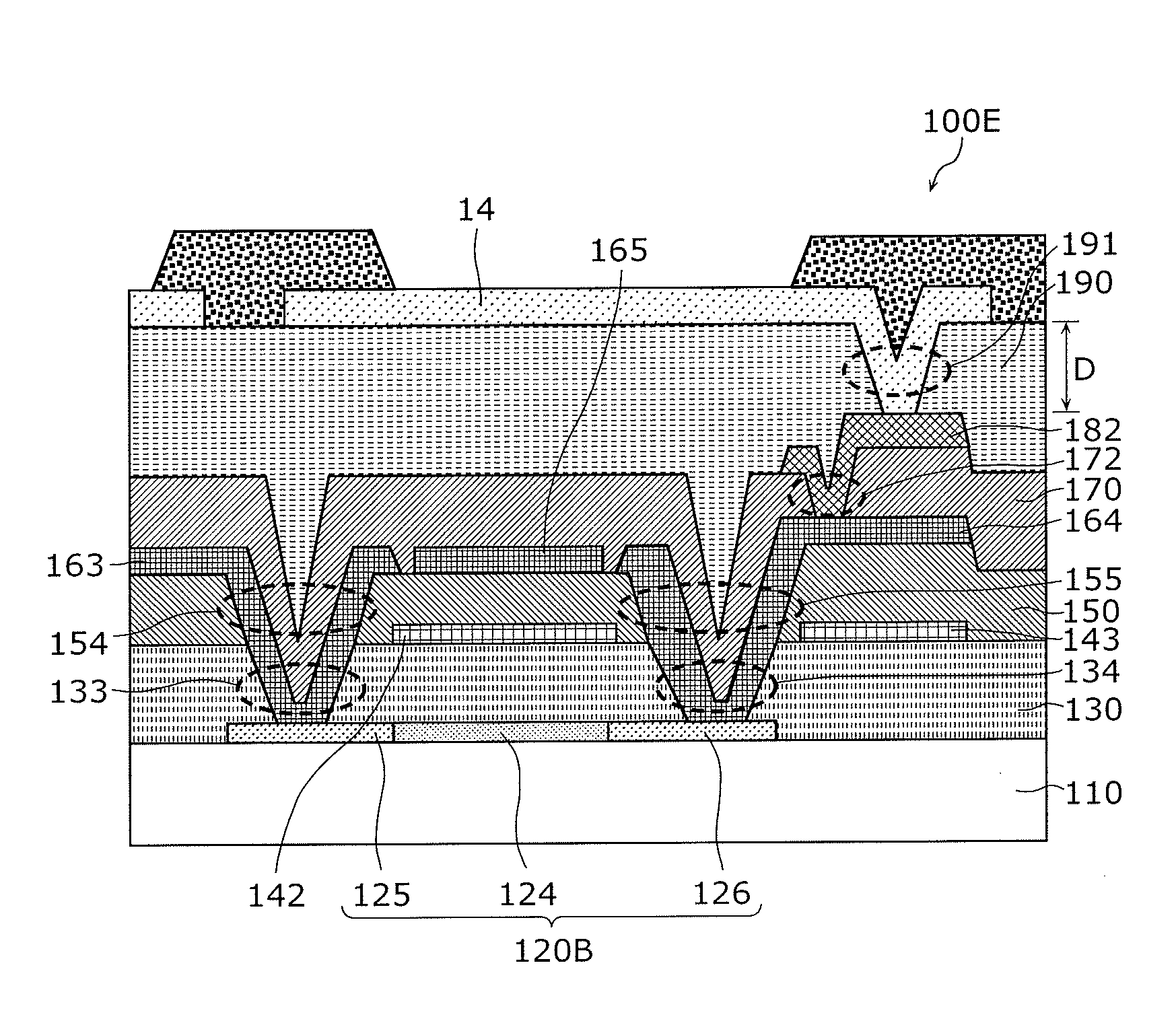
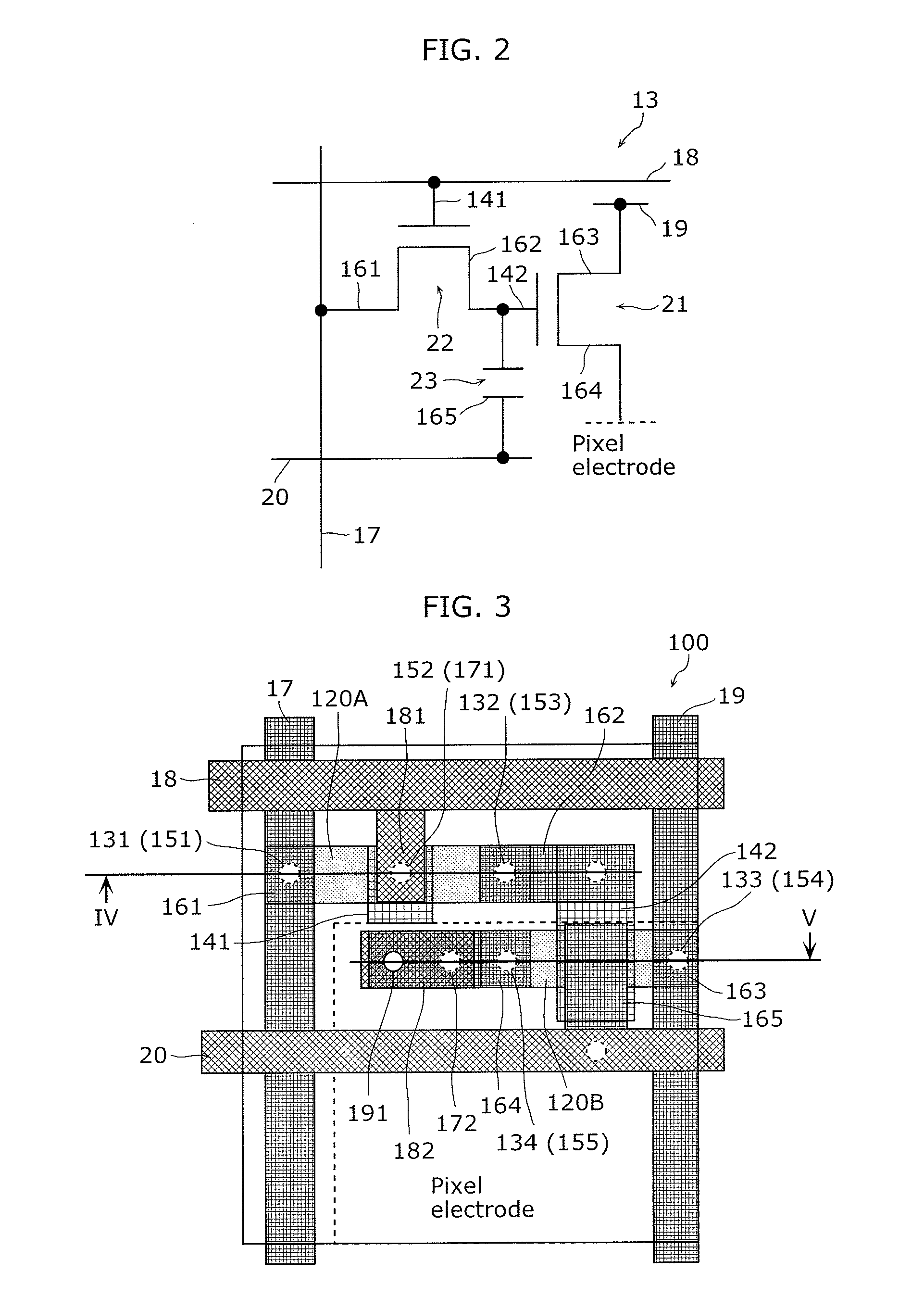
[0094]First, an example in which a semiconductor device according to Embodiment 1 of the present invention is applied to an organic EL display apparatus shall be described with reference to FIG. 1. FIG. 1 is a partial cut-out perspective view of an organic EL display apparatus according to Embodiment 1.
[0095]As shown in FIG. 1, an organic EL display apparatus 10 includes: an active-matrix substrate (TFT array substrate) 11; pixels 12 arranged in a matrix in the active-matrix substrate 11; pixel circuits 13 arranged in an array above the active-matrix substrate 11, and each connected to a corresponding one of the pixels 12; a pixel electrode 14 sequentially stacked above the pixels 12 and the pixel circuits 13; an organic EL layer 15; a common electrode 16; and source lines 17 and gate lines 18 which connect the respective pixel circuits 13 and a control circuit (not shown in the figure). The organic EL layer 15 is formed through the stacking of individual layers such as an electron ...
embodiment 2
[0178]Next, a semiconductor device according to Embodiment 2 of the present invention shall be described with reference to FIG. 17 and FIG. 18. FIG. 17 is a diagram showing a circuit configuration of a pixel circuit of a liquid-crystal display apparatus. FIG. 18 is a plan view of a semiconductor device 200 according to Embodiment 2.
[0179]As shown in FIG. 17, the semiconductor device 200 includes a transistor 31, a capacitor 32, a gate line 33, a source line 34, and a common line 3. In addition, a gate electrode 241 is connected to the gate line 33; a source electrode 261 is connected to the source line 34; a drain electrode 262 is connected to the pixel electrode and the electrode on one side of the capacitor 32; and a common electrode 35 is connected to the electrode on the other side of the capacitor 32.
[0180]In this configuration, when a gate signal is inputted to the gate line 33 and the transistor 31 is placed in the ON state, the signal voltage supplied via the source line 34 ...
PUM
 Abstract
Description
Claims
Application Information
 - R&D
- Intellectual Property
- Life Sciences
- Materials
- Tech Scout
- Unparalleled Data Quality
- Higher Quality Content
- 60% Fewer Hallucinations
Browse by: Latest US Patents, China's latest patents, Technical Efficacy Thesaurus, Application Domain, Technology Topic, Popular Technical Reports.
© 2025 PatSnap. All rights reserved.Legal|Privacy policy|Modern Slavery Act Transparency Statement|Sitemap|About US| Contact US: help@patsnap.com


