
Enhancement-depletion mode inverter with two transistor architectures

a transistor and architecture technology, applied in the direction of transistors, semiconductor devices, electrical equipment, etc., can solve the problems of device processing, difficult to perform transistor component alignment across typical substrate widths up to one meter or more, and the impact of traditional photolithographic processes and equipmen

Active Publication Date: 2016-05-05
EASTMAN KODAK CO
View PDF1 Cites 13 Cited by
  • Summary
  • Abstract
  • Description
  • Claims
  • Application Information

AI Technical Summary

Benefits of technology

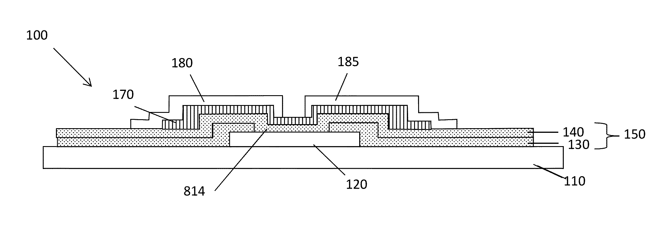
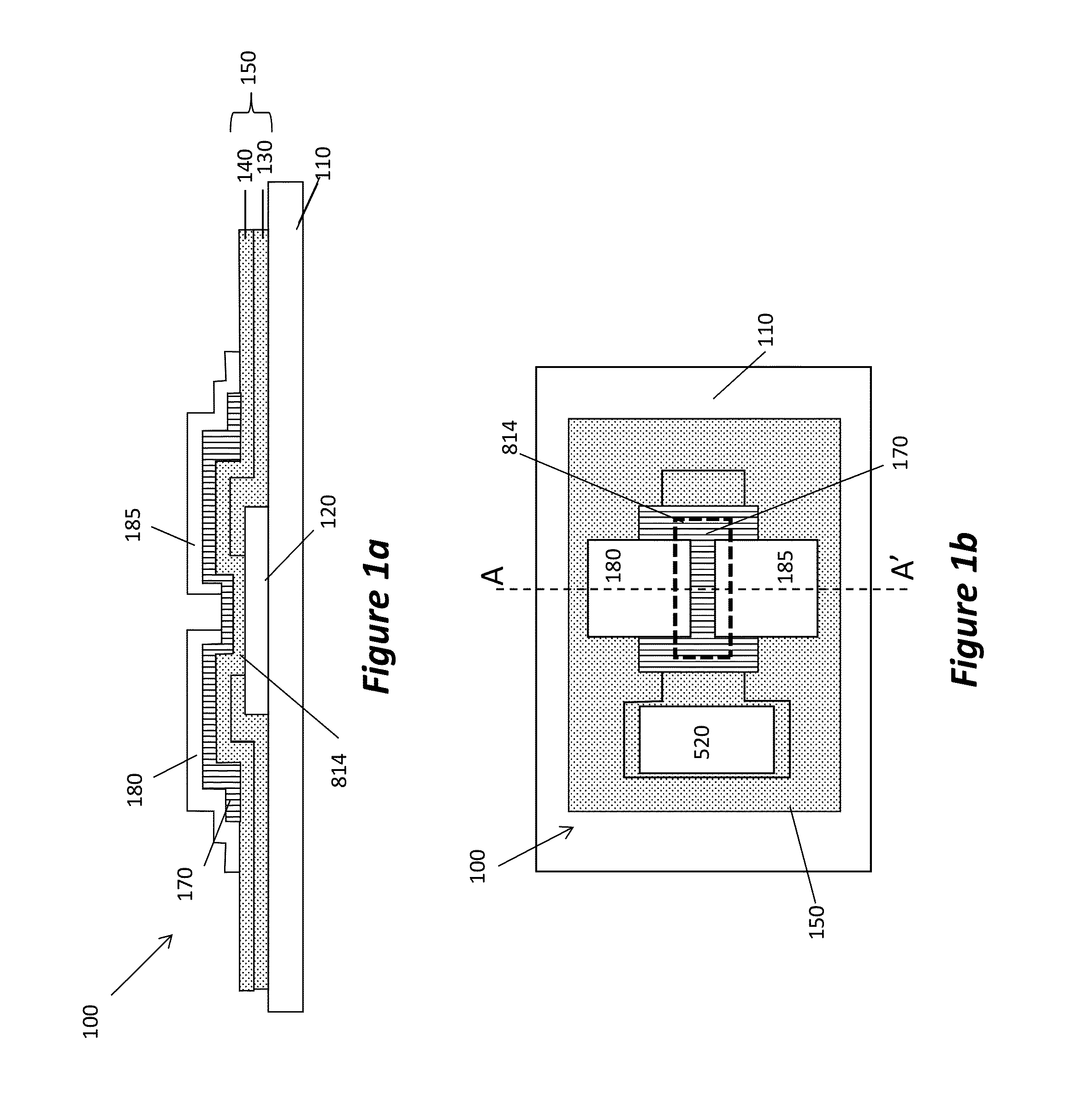
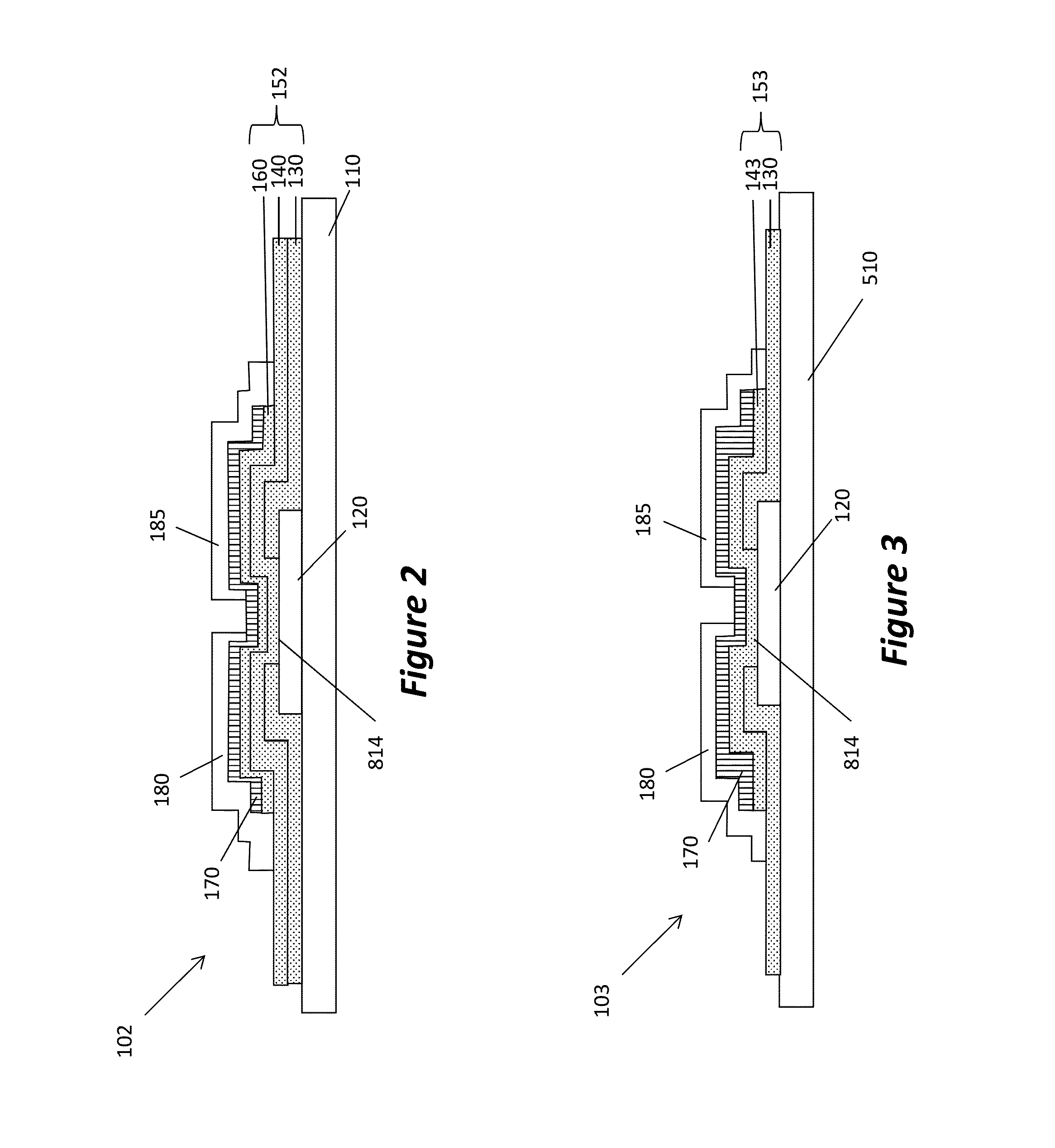
The present invention provides a variable thickness dielectric layer in a TFT that can be sized independently of other elements in the TFT, such as the source and drain. This allows for better control over the gate electrode and semiconductor layer interface, which is critical for the function of the TFT. The variable thickness dielectric layer can be used in both top gate and bottom gate structures, and can be used in either a bottom gate or top gate architecture. It also allows for better shorting and decreases gate leakage. The additional dielectric buffer layer helps to control the interface between the semiconductor and the gate dielectric, and prevents disturbances in the interface caused by the removal of the deposition inhibiting material. Overall, the invention provides a more efficient and effective method for forming TFTs with variable thickness dielectric layers.

Problems solved by technology

Plastics, however, typically limit device processing to below 200° C. There are other many issues associated with plastic supports when using traditional photolithography during conventional manufacturing, making it difficult to perform alignments of transistor components across typical substrate widths up to one meter or more.
Traditional photolithographic processes and equipment may be seriously impacted by the substrate's maximum process temperature, solvent resistance, dimensional stability, water, and solvent swelling, all key parameters in which plastic supports are typically inferior to glass.
There persists a problem of combining multiple SAD steps to form working devices.
This required layer thickness typically requires long processing times and limits the functionality of field effect devices.
In CMOS circuitry, inverters are typically easy to design but disadvantageously expensive to produce and utilize complicated production processes.
It is possible to build all NMOS or PMOS inverters, however particularly for enhancement-depletion mode circuits there are challenges to independently controlling the behavior of each transistor in the inverter circuit.
Typically, the depletion mode transistor will have a thicker semiconductor layer than the enhancement mode transistor, increasing process complexity and increasing cost.
Other alternatives include using dual gate architectures or multilayer semiconductor stacks, which have similar issues of process complexity and cost.

Method used


Image

  • Enhancement-depletion mode inverter with two transistor architectures
  • Enhancement-depletion mode inverter with two transistor architectures
  • Enhancement-depletion mode inverter with two transistor architectures

Examples


examples

General Conditions for the Preparation of Layers Using Atmospheric Pressure ALD

[0130]The preparation of a thin film coating of the material layers on glass substrates as used in the examples is described below. The ALD coating device used to prepare these layers, namely aluminum oxide, ZnO:N, and Al-doped ZnO (AZO), has been described in detail in US Patent Application Publication No. US 2009 / 0130858, the disclosure of which is herein incorporated by reference in its entirety. The coating device has an output face (facing up) that contains spatially separated elongated gas channels and operates on a gas bearing principle. The coating device can be understood with respect to delivery head 900 shown in FIG. 28. Each gas channel is composed of an output slot 95, 93, 92 which supplies gas to the output face 905, and adjacent exhaust slots 91 which remove gas from the output face 905. The order of the gas channels is P-O-P-M-P-O-P-M-P-O-P where P represents a purge channel, O represents ...

example i1

Inventive Example I1

[0139]Bottom Gate TFT with an Extra 500 Å Outside of the Channel Region

[0140]Inventive Example I1 is a bottom-gate transistor with the variable thickness dielectric stack of the present invention. Inventive Example E1 was fabricated as Comparative Example C1 with the following exceptions. After removing the PVP used to pattern the gate, a 500 Å extra dielectric layer having a gate via was formed using selective area deposition. The transistors were completed and characterized as in comparative example C1 . The performance data for Inventive Example I2 can be found in the Id-Vg curve shown in FIG. 29.

[0141]As can be seen in FIG. 29, the inventive examples having the extra dielectric outside of the channel region perform similarly to the comparative example without the extra dielectric layer, having the same gate dielectric thickness within the channel region.

All-Enhancement-Mode Inverters

[0142]In order to further probe the usefulness of the variable thickness diel...

##ventive example 13

Inventive Example 13

[0147]Inverter with Variable Thickness Dielectric Stack

[0148]Inventive example I3, was prepared as comparative example C1 with the following exception. After removing the PVP used to pattern the gate, a 250 Å extra dielectric layer having a gate via was formed using selective area deposition (as in Inventive Example I1). The pattern is chosen so that the inverters have the variable dielectric stack illustrated in FIGS. 22a and 22b. This results in inverters of Inventive Example I3 having drive TFTs with a total gate dielectric thickness of 500 Å, and the load TFT having a total gate dielectric thickness of 750 Å. The drive transistors for each inverter had as designed W=6 pixel / L=1 pixel, and the load transistors for each inverter had an as designed W=3 pixel / L=3 pixel. The circuit was characterized as in Comparative example C2, and the frequency, time per stage, and fraction of the peak-to-peak swing for Vdd=16 V can be found in Table 2.


PUM


Abstract

An enhancement-depletion-mode inverter includes a load transistor and a drive transistor. The load transistor has a top gate architecture with a first source, a first drain, a load channel region, a first semiconductor layer, and a first gate electrode. A load gate dielectric is in the load channel region, and has a load dielectric thickness. The load transistor is configured to operate in a depletion mode. The drive transistor has a bottom gate architecture with a second source, a second drain, a drive channel region, a second semiconductor layer, and a second gate electrode. A drive gate dielectric is in the drive channel region, and has a drive dielectric thickness that is different from the load dielectric thickness. The drive transistor is configured to operate in a normal mode or an enhancement mode. The first source is electrically connected to the second drain and the first gate.

Description

CROSS REFERENCE TO RELATED APPLICATIONS[0001]Reference is made to commonly-assigned, U.S. patent application Ser. No. ______ (Docket K001871), entitled “TFT SUBSTRATE WITH VARIABLE DIELECTRIC THICKNESS”, Ser. No. ______ (Docket K001895), entitled “METHOD FOR FORMING A VARIABLE THICKNESS DIELECTRIC STACK”, Ser. No. ______ (Docket K001897), entitled “ENHANCEMENT MODE INVERTER WITH VARIABLE THICKNESS DIELECTRIC STACK”, all filed concurrently herewith.FIELD OF THE INVENTION[0002]This invention relates generally to patterned thin film fabrication and electronic and optoelectronic devices including patterned thin films. In particular, this invention relates to selective area deposition of materials including, for example, metal-oxides and devices including, for example, thin film transistors, inverters and circuits produced using, for example, this fabrication technique.BACKGROUND OF THE INVENTION[0003]Modern-day electronics require multiple patterned layers of electrically or optically a...

Claims


Application Information

Patent Timeline
IPC IPC(8): H01L27/088H01L29/786
CPCH01L29/7869H01L27/0883H01L27/1251H01L27/1225
Inventor ELLINGER, CAROLYN RAENELSON, SHELBY FORRESTER
Owner EASTMAN KODAK CO
Learn More