
Multi-channel gate-all-around fet

a gate-all-around, multi-channel technology, applied in the direction of electrical equipment, nanotechnology, semiconductor devices, etc., can solve the problem of short circuit between the source and drain region

Active Publication Date: 2016-04-21
TAIWAN SEMICON MFG CO LTD
View PDF2 Cites 45 Cited by
  • Summary
  • Abstract
  • Description
  • Claims
  • Application Information

AI Technical Summary

Benefits of technology

The patent describes a new way to make semiconductors that can perform better and at lower voltages. The method uses vertical silicon nanowires instead of the traditional fin structure in conventional devices. Problems with existing nanowire devices can occur when a conductive material is used to form the gate, which can cause short circuits between the source and drain regions. The new method avoids this issue by forming insulating barriers in contact with the source and drain regions and using a temporary gate structure. This leads to a more reliable and high-performing device. The fabrication process is also more cost-effective because it uses sacrificial films for self-alignment.

Problems solved by technology

One problem that occurs in existing nanowire GAA FETs is that, when a conductive material is used to form the wrap-around gate, a short circuit can develop between the source and drain regions and the conductive gate portion that underlies the channel.

Method used


Image

  • Multi-channel gate-all-around fet
  • Multi-channel gate-all-around fet
  • Multi-channel gate-all-around fet

Examples


Embodiment Construction

[0020]In the following description, certain specific details are set forth in order to provide a thorough understanding of various aspects of the disclosed subject matter. However, the disclosed subject matter may be practiced without these specific details. In some instances, well-known structures and methods of semiconductor processing comprising embodiments of the subject matter disclosed herein have not been described in detail to avoid obscuring the descriptions of other aspects of the present disclosure.

[0021]Unless the context requires otherwise, throughout the specification and claims that follow, the word “comprise” and variations thereof, such as “comprises” and “comprising” are to be construed in an open, inclusive sense, that is, as “including, but not limited to.”

[0022]Reference throughout the specification to “one embodiment” or “an embodiment” means that a particular feature, structure, or characteristic described in connection with the embodiment is included in at le...


PUM


Abstract

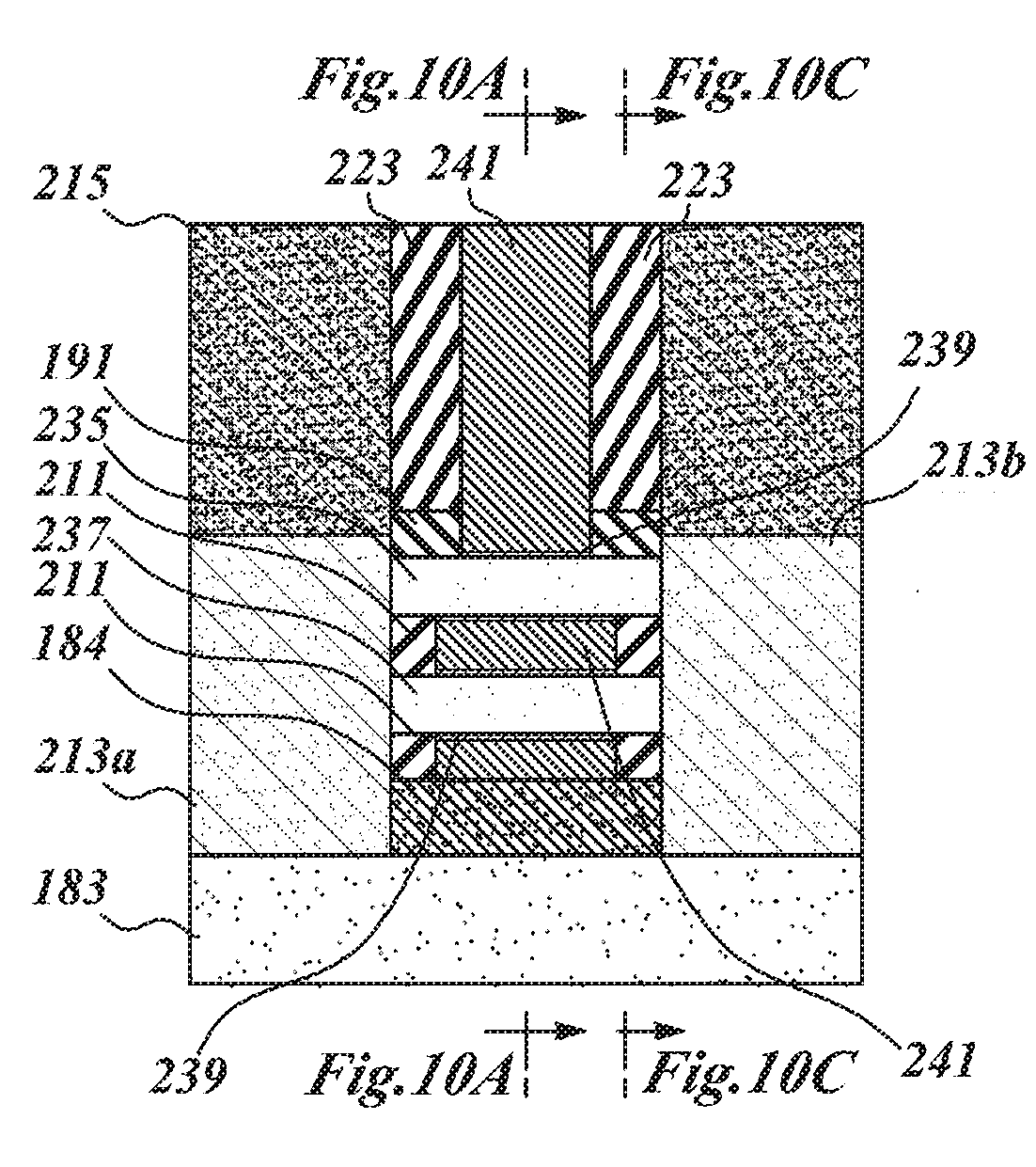
A high performance GAA FET is described in which vertically stacked silicon nanowires carry substantially the same drive current as the fin in a conventional FinFET transistor, but at a lower operating voltage, and with greater reliability. One problem that occurs in existing nanowire GAA FETs is that, when a metal is used to form the wraparound gate, a short circuit can develop between the source and drain regions and the metal gate portion that underlies the channel. The vertically stacked nanowire device described herein, however, avoids such short circuits by forming insulating barriers in contact with the source and drain regions, prior to forming the gate. Through the use of sacrificial films, the fabrication process is almost fully self-aligned, such that only one lithography mask layer is needed, which significantly reduces manufacturing costs.

Description

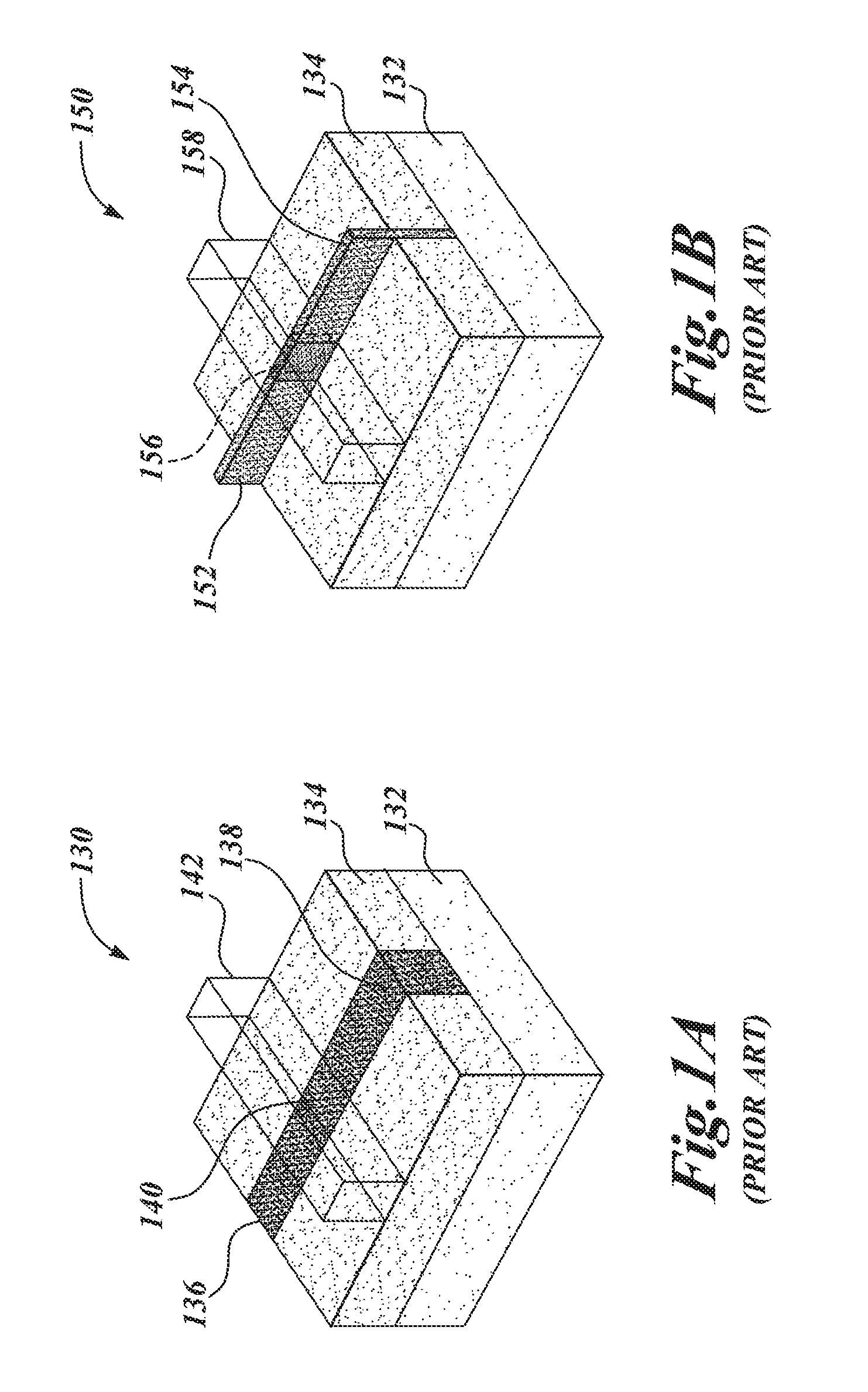
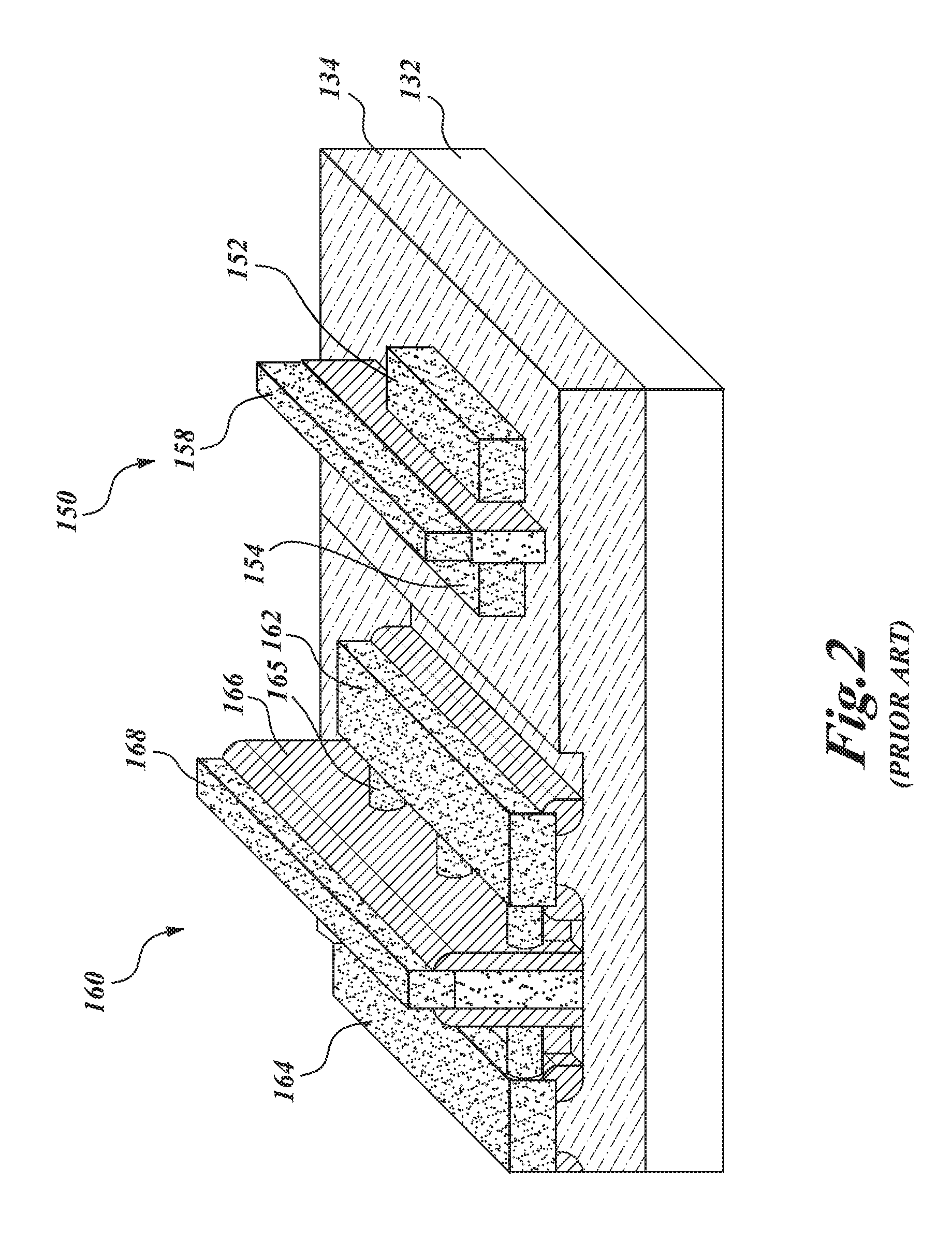
CROSS REFERENCE TO RELATED APPLICATION[0001]This patent application is a divisional of U.S. patent application Ser. No. 14 / 312,418 filed Jun. 23, 2014, which application is hereby incorporated by reference in its entirety.BACKGROUND[0002]1. Technical Field[0003]The present disclosure generally relates to field effect transistor (FET) structures with wrap-around gates and, in particular, to a high performance multi-channel gate-all-around FET.[0004]2. Description of the Related Art[0005]Conventional integrated circuits incorporate 2-D planar field effect transistors (FETs) in which current flows through a semiconducting channel between a source and a drain, in response to a voltage applied to a control gate. To provide better control of the current flow, 3D transistors have also been developed. A 3D transistor structure is shown and described below in comparison with a traditional 2-D planar transistor. A 3D transistor is an electronic switching device in which the planar semiconduct...

Claims


Application Information

Patent Timeline
Patent Type & Authority Applications(United States)
IPC IPC(8): H01L29/423H01L29/165H01L29/06H01L29/16H01L29/786H01L29/66
CPCH01L29/42392H01L29/78696H01L29/78618H01L29/66742H01L29/165H01L29/0649H01L29/0673H01L29/1608H01L29/66545B82Y10/00H01L29/66439H01L29/775H01L29/66772H01L29/42364H01L29/785H01L29/518H01L29/51H01L29/6681H01L29/167H01L29/36H01L29/1037H01L29/161
Inventor LIU, QINGXIE, RUILONGYEH, CHUN-CHENCAI, XIUYU
Owner TAIWAN SEMICON MFG CO LTD
Learn More