
Latch initialization for a data storage device

a data storage device and initialization technology, applied in the field of data storage devices, can solve the problems of affecting the performance of a memory device, and the storage elements of a flash memory device may be more prone to cross-coupling effects, so as to reduce the effect of leakage current and/or read disturb effects

Active Publication Date: 2016-04-07
SANDISK TECH LLC
View PDF0 Cites 5 Cited by
  • Summary
  • Abstract
  • Description
  • Claims
  • Application Information

AI Technical Summary

Benefits of technology

The patent describes a method to avoid programming a common value to a memory, which can cause leakage current and read disturb effects. This is done by using a set of bits with multiple values to initialize the memory, which ensures that a randomized bit sequence or pattern is used instead of a common value. This method can be particularly useful when a memory has a multi-level cell configuration and stores multiple logical pages. The technical effect of this patent is to improve the reliability and efficiency of the memory system by reducing leakage current and read disturb effects.

Problems solved by technology

Storing a common value in multiple adjacent storage elements can degrade performance of a memory device, such as by causing a large leakage current in some memory devices.
Further, storing a common value in multiple adjacent storage elements can cause disturb effects in some memory devices.
For example, storage elements of a flash memory device may be more prone to cross-coupling effects (and thus read errors and decoding errors) if adjacent storage elements are programmed to a common value.
However, sending the dummy data from a controller to a memory may use a large amount of resources at a memory device (e.g., by using power to transfer the dummy data over a bus between the controller and the memory).

Method used


Image

  • Latch initialization for a data storage device
  • Latch initialization for a data storage device
  • Latch initialization for a data storage device

Examples


Embodiment Construction

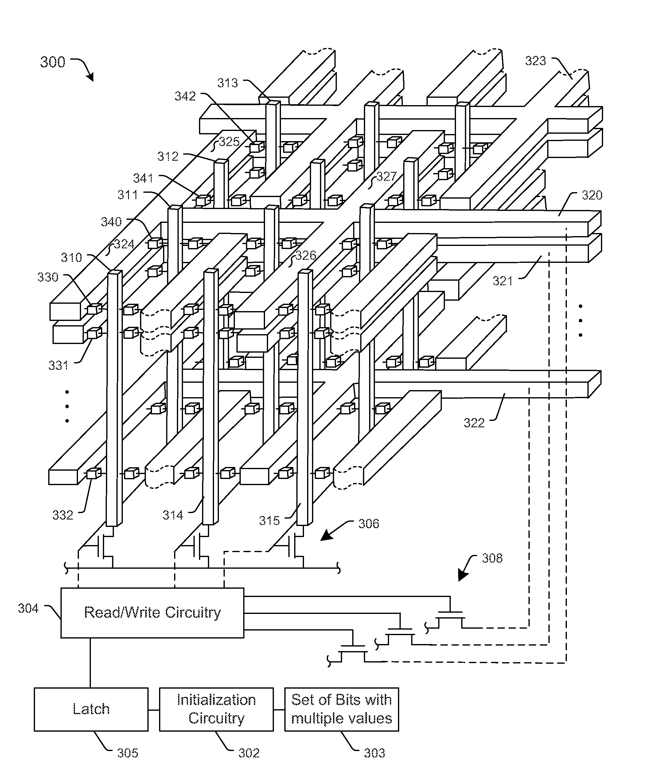
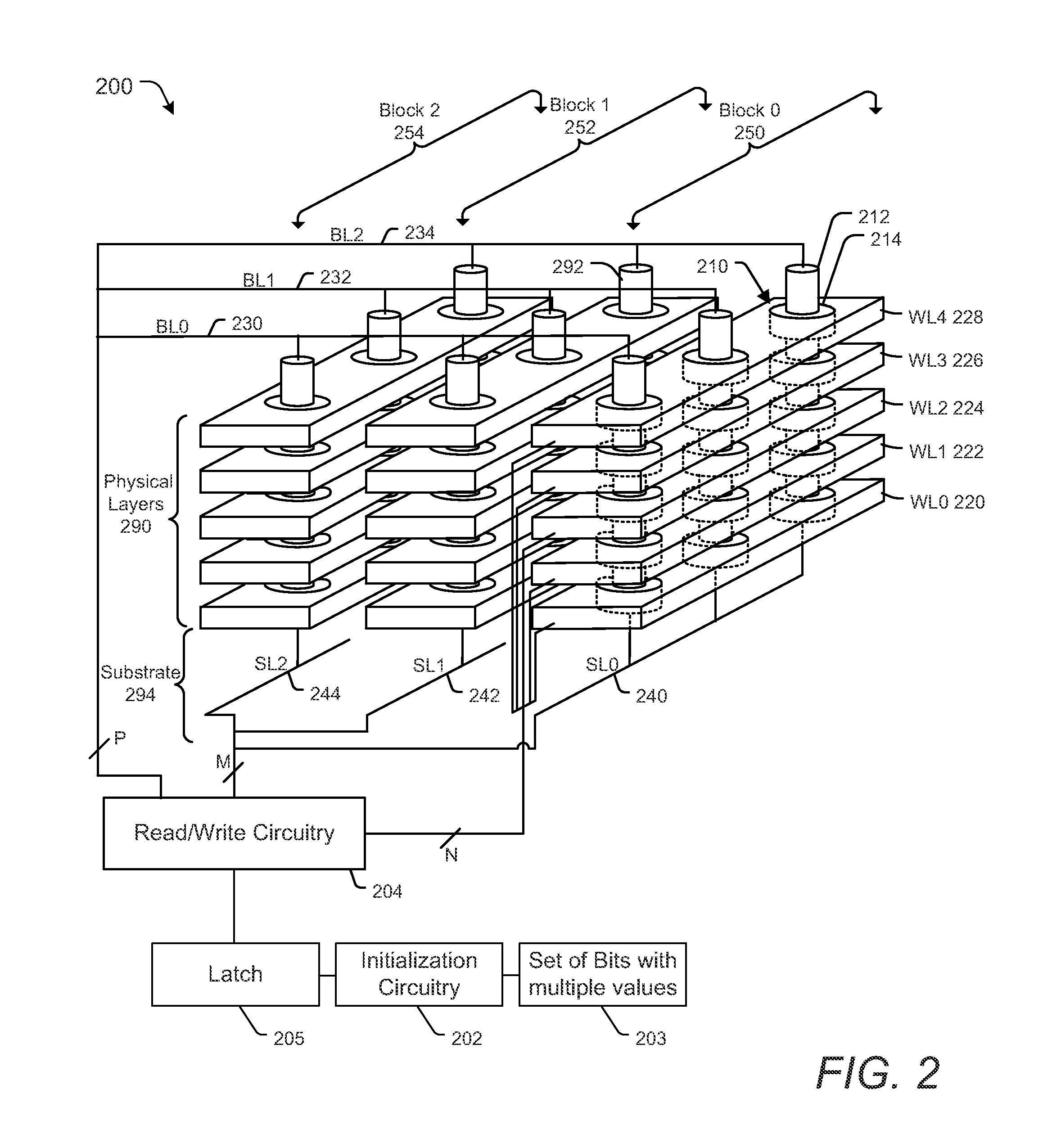
[0011]A write process used by a non-volatile memory may use a multi-stage write process to write a page of data to the non-volatile memory. For example, the write process may include sending (e.g., by a memory controller or by a host computer) a write opcode to the memory die. The memory die may initialize a page-size volatile latch for receiving data to be written to the non-volatile memory. For example, the initialization may set all bits of the latch to a logic “1” state or to a logic “0” state. In some implementations, initializing the latch is performed after sending a destination address associated with the data to the memory die.

[0012]The memory controller or host computer may send one or more bytes specifying the address of the write operation. The address may include two elements: an identification of the page to be written (e.g., die number, plane number within the die, block number within the plane, and / or page number within the block) and an identification of the start l...


PUM


Abstract

A data storage device may include a memory die. The memory die includes a memory and a latch. A method may include receiving a command corresponding to a write operation to write information to the memory. The method may further include loading a set of bits into the latch prior to receiving the information at the memory die. The set of bits includes at least a first bit having a first value and a second bit having a second value that is different than the first value. The method further includes receiving the information at the memory die and overwriting at least a portion of the set of bits at the latch with the information.

Description

FIELD OF THE DISCLOSURE[0001]The present disclosure is generally related to data storage devices and more particularly to latch initialization for data storage devices.BACKGROUND[0002]Non-volatile data storage devices have enabled increased portability of data and software applications. For example, multi-level cell (MLC) storage elements of a memory device may each store a value indicating multiple bits of data, enhancing data storage density as compared to single-level cell (SLC) memory devices. Consequently, memory devices may enable users to store and access a large amount of data. In some cases, the data may include sequences of consecutive values (e.g., a string of logic “0” values or a string of logic “1” values).[0003]Storing a common value in multiple adjacent storage elements can degrade performance of a memory device, such as by causing a large leakage current in some memory devices. To illustrate, in a resistive-random access memory (ReRAM), programming a column of stora...

Claims


Application Information

Patent Timeline
Patent Type & Authority Applications(United States)
IPC IPC(8): G11C16/20G11C11/56
CPCG11C11/5671G11C16/20G11C7/1006G11C7/1009G11C7/1087G11C11/5614G11C11/5628G11C13/0033G11C13/0069G11C16/10G11C16/3427G11C7/20
Inventor LASSER, MENAHEM
Owner SANDISK TECH LLC
Learn More