Method for manufacturing light-emitting device packages, light-emitting device package strip, and light-emitting device package

a technology of light-emitting devices and packaging, which is applied in the manufacture of electric discharge tubes/lamps, lighting and heating apparatus, and discharge tubes luminescnet screens. it can solve the problems of reducing productivity, increasing the price of products, and requiring a lot of time and cost for packaging processes, so as to reduce the price of products and improve productivity. , the effect of simple process

Active Publication Date: 2016-02-25
LUMENS
View PDF12 Cites 20 Cited by
  • Summary
  • Abstract
  • Description
  • Claims
  • Application Information

AI Technical Summary

Benefits of technology

[0010]The present invention provides a method capable of manufacturing a large number of light-emitting device packages through a simple process, reducing the price of products, improving productivity, manufacturing small and thin products, and lowering a performance difference among manufactured products.

Problems solved by technology

However, according to the above conventional light-emitting device package manufacturing method, since light-emitting devices are separately mounted on substrates and a reflective member and an optical conversion member are formed on each of the light-emitting devices, a lot of time and cost are required for a packaging process, the price of products are increased, and thus productivity is reduced.
As such, the manufactured light-emitting device packages have a relatively large size or thickness and thus small and thin products cannot be manufactured.
Furthermore, according to the conventional light-emitting device package manufacturing method, since optical members are separately provided on light-emitting devices, a performance difference occurs among the manufactured light-emitting device packages.

Method used


Image

  • Method for manufacturing light-emitting device packages, light-emitting device package strip, and light-emitting device package
  • Method for manufacturing light-emitting device packages, light-emitting device package strip, and light-emitting device package
  • Method for manufacturing light-emitting device packages, light-emitting device package strip, and light-emitting device package

Examples


Embodiment Construction

[0064]Hereinafter, the present invention will be described in detail by explaining embodiments of the invention with reference to the attached drawings.

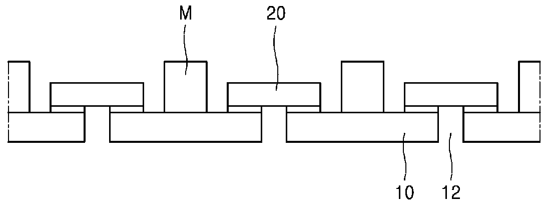
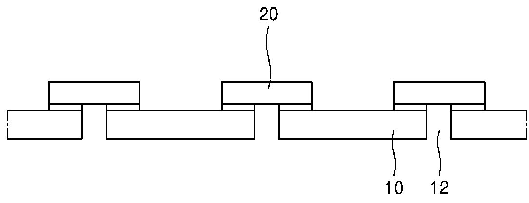
[0065]A chip scale package (CSP) is a high power package regarded as a next-generation light source in addition to a wafer level package (WLP), a laminated ceramic package, a multi-chip package, a metal package, and a chip on board (COB). Compared to conventional light-emitting device packages, the CSP is producible in a small size at a high density. As such, the CSP may be produced at a low cost through a simple process, and have a high heat resistance and an excellent color uniformity.

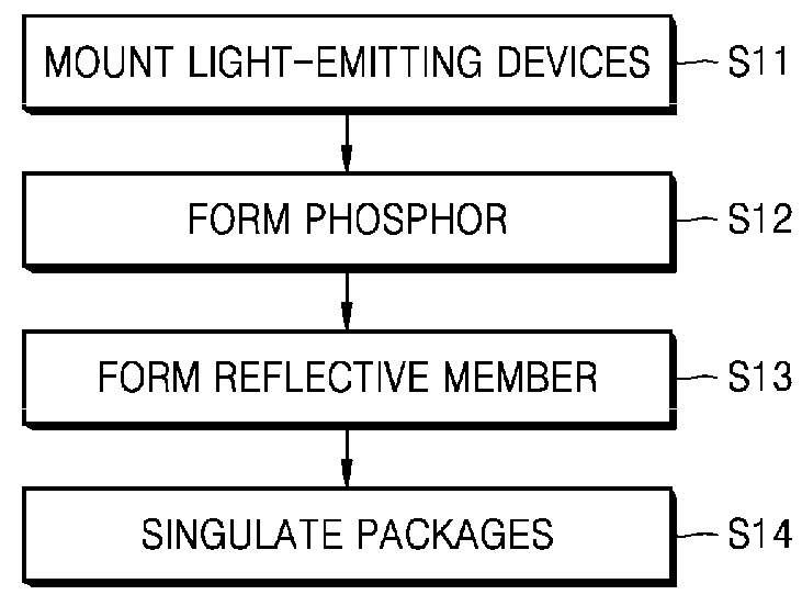
[0066]The CSP corresponds to a technology of providing a light-emitting device package on a chip scale, and is characterized in that a large number of light-emitting devices are mounted on a substrate strip, a phosphor is coated simultaneously on the light-emitting devices, and then packages are singulated.

[0067]Accordingly, the CSP has a size similar...


PUM


Abstract

Disclosed is a method for manufacturing a chip scale package (CSP) for a light-emitting diode (LED). The method may include a light-emitting device mounting step for mounting a plurality of light-emitting devices on a substrate strip, a phosphor forming step for forming a phosphor on the plurality of light-emitting devices, a reflective member forming step for forming a reflective member on the substrate strip to surround the phosphor, and a package singulation step for singulating unit packages by cutting the substrate strip and the reflective member.

Description

CROSS-REFERENCE TO RELATED PATENT APPLICATION[0001]This application claims the benefit of Korean Patent Application Nos. 10-2014-0108346, filed on Aug. 20, 2014, 10-2014-0164363, filed on Nov. 24, 2014, and 10-2014-0164364, filed on Nov. 24, 2014, in the Korean Intellectual Property Office, respectively, the disclosure of which is incorporated herein in its entirety by reference.BACKGROUND[0002]1. Field[0003]The present invention relates to a method for manufacturing light-emitting device packages, a light-emitting device package strip, and a light-emitting device package and, more particularly, to a method for manufacturing light-emitting device packages usable in a display apparatus or a lighting apparatus, a light-emitting device package strip, and a light-emitting device package.[0004]2. Description of the Related Art[0005]A light-emitting diode (LED) refers a type of semiconductor element capable of displaying light of various colors by providing a light-emitting source using a...

Claims


Application Information

Patent Timeline
Patent Type & Authority Applications(United States)
IPC IPC(8): H05B33/22F21S4/00H05B33/10
CPCH05B33/22F21S4/006H05B33/10H01L33/50H01L33/60H01L33/62H01L2933/0033H01L2933/0041H01L2933/0066F21S4/24F21S4/20
Inventor OH, SEUNG HYUNLEE, SEUNG HOONYUN, SUNG YOLELIM, JUNG AJO, SUNG SIKKIM, IN SOOYOO, TAE KYOUNG
Owner LUMENS
Why Eureka
Try Eureka