Manufacturing process of the thermoelectric conversion element
a technology of thermoelectric conversion element and manufacturing process, which is applied in the manufacture/treatment of thermoelectric devices, thermoelectric device junction materials, electrical apparatus, etc., can solve the problems of reducing the conversion efficiency, the inability to boost the thermoelectric figure of merit unlimitedly, and the need for rare earth elements has become an urgent need, so as to reduce the need of rare earth elements, the cost can be effectively reduced, and the need of thermoelectric merit is reduced.
- Summary
- Abstract
- Description
- Claims
- Application Information
AI Technical Summary
Benefits of technology
Problems solved by technology
Method used
Image
Examples
first embodiment
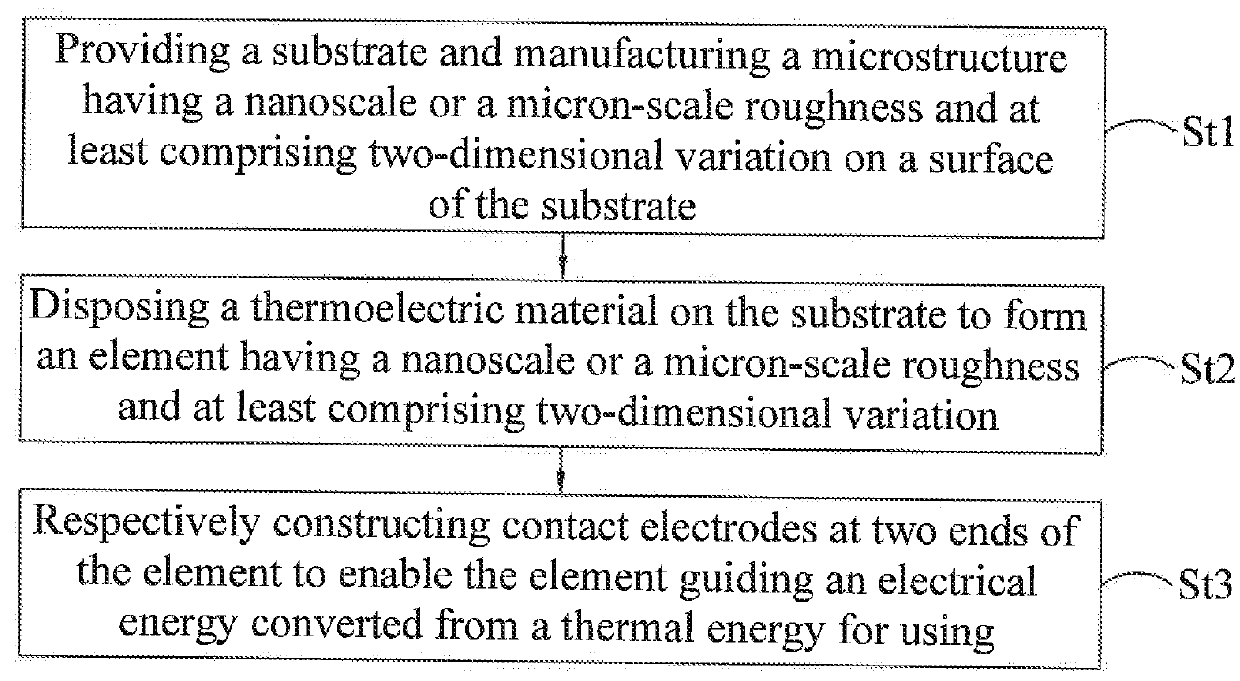
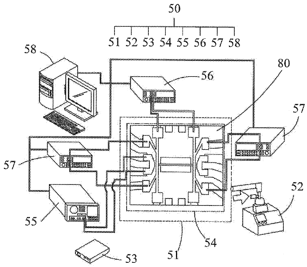
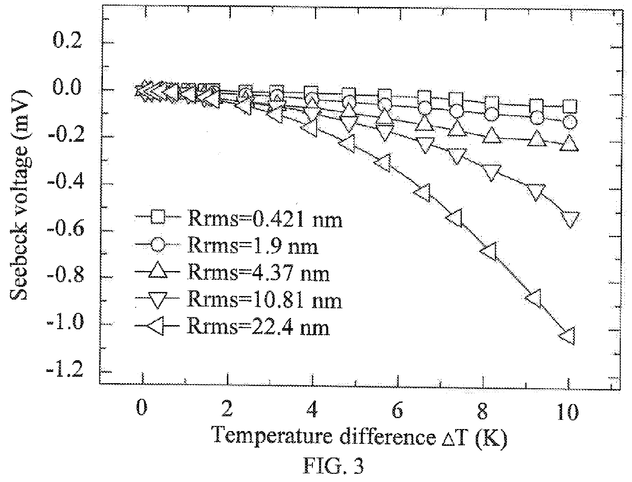
[0059]Please refer to FIG. 3 which is an experimental data diagram of a manufacturing process of a thermoelectric conversion element of the present invention. The steps of the manufacturing process disclosed in the present invention are used to manufacture the nickel nanowire having diverse nanoscale surface roughness, and the measuring system 50 shown in FIG. 2 is used to conduct measurements of the related data.
[0060]The experimental result shows that as the roughness of the nickel nanowire is controlled within the nanoscale, conductivity thereof will not greatly decrease owing to the roughness. The nickel nanowire having the largest surface roughness has higher thermoelectric effect by a multiple of 4.5 than that of the nickel nanowire having the least surface roughness. Under the circumstances of the temperature difference for two ends of the nanowire is about 10.068K; the thermal electromotive force is up to 0.791 mV.
[0061]The reason can be inferred to that the technique disclo...
third embodiment
[0077]Please refer to FIG. 7 which is an experimental data diagram of a manufacturing process of a thermoelectric conversion element of the present invention. For example, the present embodiment uses an anodic aluminum oxide (AAO) as the porous substrate to construct the porous thermoelectric thin film 200 having different thicknesses (30-80 nm) and being made of metal material, wherein the intervals between a plurality of holes of the AAO substrate are 20 nm.
[0078]It can be found through the experimental result that the measured thermoelectric voltage of the porous thermoelectric thin film 200 disposed on the AAO substrate is clearly better than the continuous thin film directly disposed on a glass substrate of a smooth surface; and the experimental result shows that the smaller thickness the porous thermoelectric thin film 200 is, the better the thermoelectric effect is.
[0079]A manufacturing process of a thermoelectric conversion element disclosed in the present invention has adva...
PUM
 Abstract
Description
Claims
Application Information
 - R&D
- Intellectual Property
- Life Sciences
- Materials
- Tech Scout
- Unparalleled Data Quality
- Higher Quality Content
- 60% Fewer Hallucinations
Browse by: Latest US Patents, China's latest patents, Technical Efficacy Thesaurus, Application Domain, Technology Topic, Popular Technical Reports.
© 2025 PatSnap. All rights reserved.Legal|Privacy policy|Modern Slavery Act Transparency Statement|Sitemap|About US| Contact US: help@patsnap.com


