Boron compound for organic electroluminescent elements, and organic electroluminescent element
a technology of electroluminescent elements and boron compounds, which is applied in the direction of organic compounds, luminescent compositions, organic chemistry, etc., can solve the problems of unsatisfactory high-efficiency light emission, and achieve the effect of reducing the voltage of the organic el device, improving light-emitting characteristics, and low lowest unoccupied molecular orbital energy level
- Summary
- Abstract
- Description
- Claims
- Application Information
AI Technical Summary
Benefits of technology
Problems solved by technology
Method used
Image
Examples
synthesis example 1
Synthesis of Compound B14
[0111]
[0112]Under a nitrogen atmosphere, 10.00 g (0.0390 mol) of a compound (A), 6.14 g (0.0195 mol) of tribromobenzene, 0.74 g of copper iodide, 24.84 g of potassium triphosphate, and 500 ml of 1,4-dioxane were loaded and stirred at room temperature. 1.34 g of trans-1,2-cyclohexanediamine was added to the mixture and the whole was stirred at 110° C. for 9 hr. The reaction solution was cooled to room temperature and filtered, followed by concentration. The resultant residue was purified by silica gel column chromatography to provide 3.00 g (0.00451 mol, yield: 12%) of an intermediate (B) as a white solid.
[0113]Under a nitrogen atmosphere, 3.00 g (0.00451 mol) of the intermediate (B), 110.41 g (0.5412 mol) of iodobenzene, 1.89 g of copper, and 6.86 g of potassium carbonate were loaded and stirred at 180° C. for 5 hr. The reaction solution was cooled to room temperature and filtered, followed by concentration. The resultant residue was purified by silica gel c...
example 1
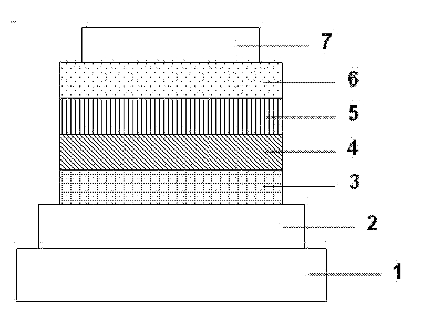
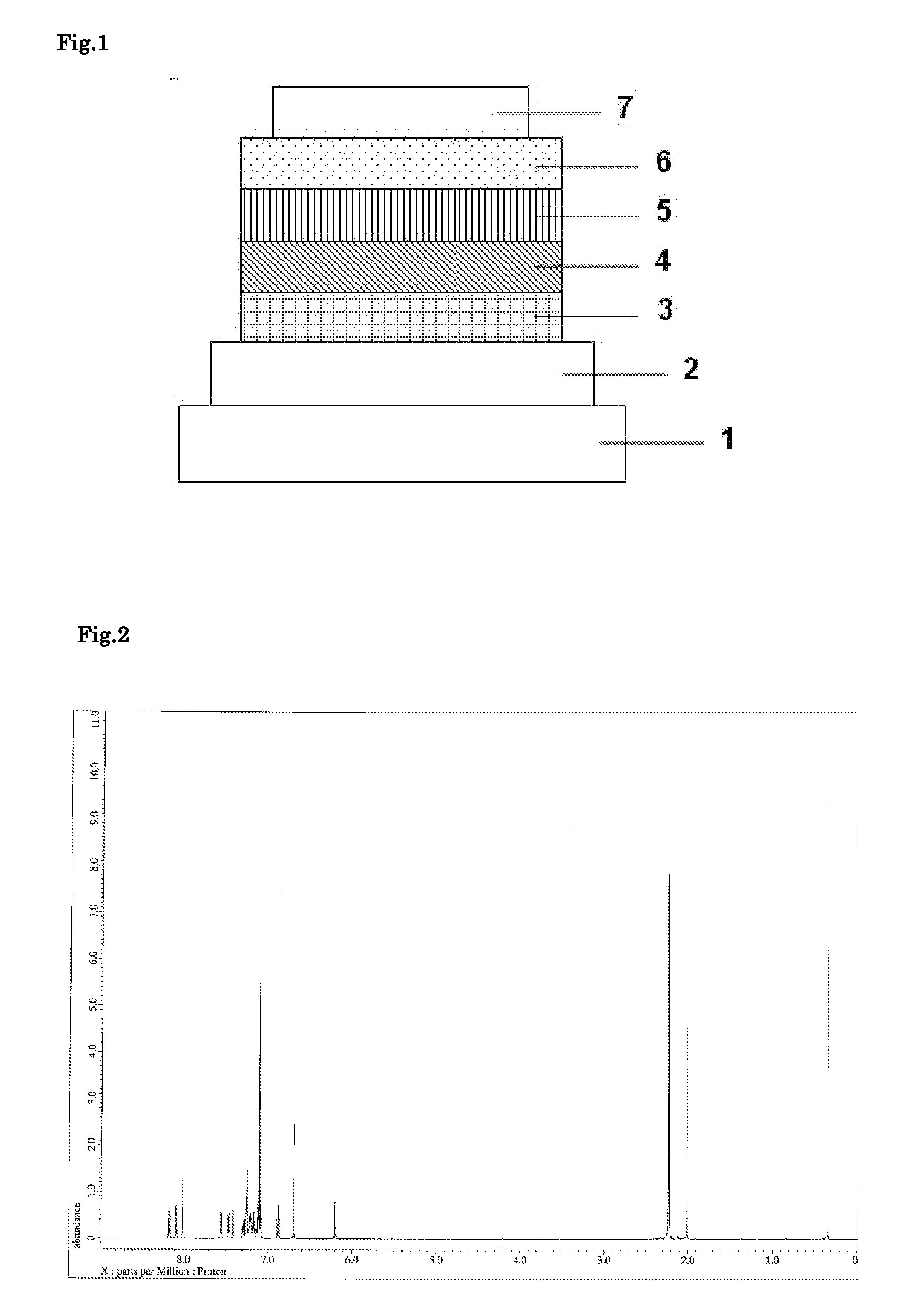
[0116]Each thin film was laminated by a vacuum deposition method at a degree of vacuum of 4.0×10⁻⁵ Pa on a glass substrate on which an anode formed of ITO having a thickness of 110 nm had been formed. First, copper phthalocyanine (CuPC) was formed into a layer having a thickness of 25 nm on the ITO. Next, 4,4′-bis[N-(1-naphthyl)-N-phenylamino]biphenyl (NPB) was formed into a layer having a thickness of 40 nm to serve as a hole-transporting layer. Next, the compound (B14) as a host material and tris(2-phenylpyridine)iridium(III) (Ir(ppy)3) as a phosphorescent light-emitting dopant were co-deposited from different deposition sources onto the hole-transporting layer to form a light-emitting layer having a thickness of 40 nm. The concentration of Ir(ppy)3 in the light-emitting layer was 10.0 wt %. Next, tris(8-hydroxyquinolinato)aluminum(III) (Alq3) was formed into a layer having a thickness of 20 nm to serve as an electron-transporting layer. Further, lithium fluoride (LiF) was formed ...
examples 2 to 12
[0118]Compounds A8, A15, A24, B5, B6, B24, C8, D37, E25, F28, and F32 were synthesized in the same manner as in Synthesis Example 1.
[0119]Organic EL devices were each produced in the same manner as in Example 1 except that the compounds A8, A15, A24, B5, B6, B24, C8, D37, E25, F28, and F32 were each used instead of the compound B14 as the host material for the light-emitting layer of Example 1. It was found that the local maximum wavelength of the emission spectrum of each of the devices was 520 nm, and hence light emission from Ir(ppy)3 was obtained. The respective light-emitting characteristics are shown in Table 1.
PUM
| Property | Measurement | Unit |
|---|---|---|
| work function | aaaaa | aaaaa |
| transmittance | aaaaa | aaaaa |
| thickness | aaaaa | aaaaa |
Abstract
Description
Claims
Application Information
 - R&D
- Intellectual Property
- Life Sciences
- Materials
- Tech Scout
- Unparalleled Data Quality
- Higher Quality Content
- 60% Fewer Hallucinations
Browse by: Latest US Patents, China's latest patents, Technical Efficacy Thesaurus, Application Domain, Technology Topic, Popular Technical Reports.
© 2025 PatSnap. All rights reserved.Legal|Privacy policy|Modern Slavery Act Transparency Statement|Sitemap|About US| Contact US: help@patsnap.com


