
Array substrate and method of fabricating the same, and liquid crystal display device

a liquid crystal display and array substrate technology, applied in semiconductor devices, semiconductor/solid-state device details, instruments, etc., can solve the problems of complex fabrication process, and achieve the effects of good conductivity, large capacitance, and simple fabrication process

Active Publication Date: 2016-01-14
BOE TECH GRP CO LTD
View PDF0 Cites 0 Cited by
  • Summary
  • Abstract
  • Description
  • Claims
  • Application Information

AI Technical Summary

Benefits of technology

This simplifies the fabrication process, enhances the driving effect by increasing the electric field intensity and capacitance, and improves light transmittance by removing the gate insulation layer between electrodes.

Problems solved by technology

Therefore, the fabricating process is complex.

Method used


Image

  • Array substrate and method of fabricating the same, and liquid crystal display device
  • Array substrate and method of fabricating the same, and liquid crystal display device
  • Array substrate and method of fabricating the same, and liquid crystal display device

Examples


first embodiment

[0049]This embodiment provides a method of fabricating an array substrate, the method comprises following steps 1 through 3.

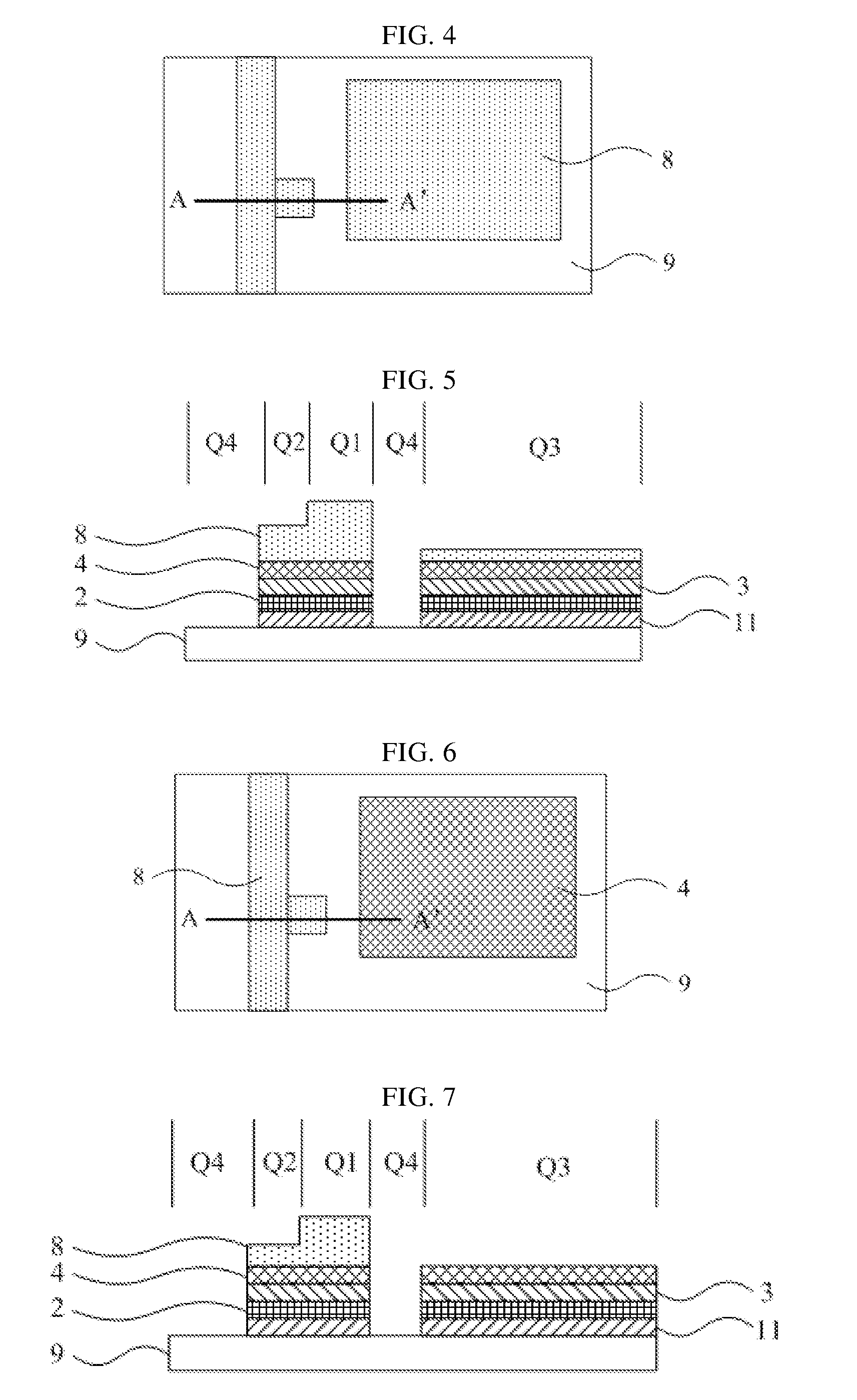
[0050]In the step 1, a first transparent conductive material layer, an insulation material layer, a semiconductor material layer and a photoresist layer are sequentially formed on a substrate base, and patterns including a gate line, a gate, a gate insulation layer, a semiconductor layer and a first transparent electrode are formed by patterning process, the gate insulation layer is formed only on the gate and the gate line.

[0051]In the step 2, a passivation layer is formed on the substrate base, and a source via and a drain via which are connected to the semiconductor layer are formed in the passivation layer.

[0052]In the step 3, a second transparent conductive material layer and a source-drain metal layer are sequentially formed on the substrate base, and patterns including a source, a drain and a second transparent electrode are formed by patterning process,...

second embodiment

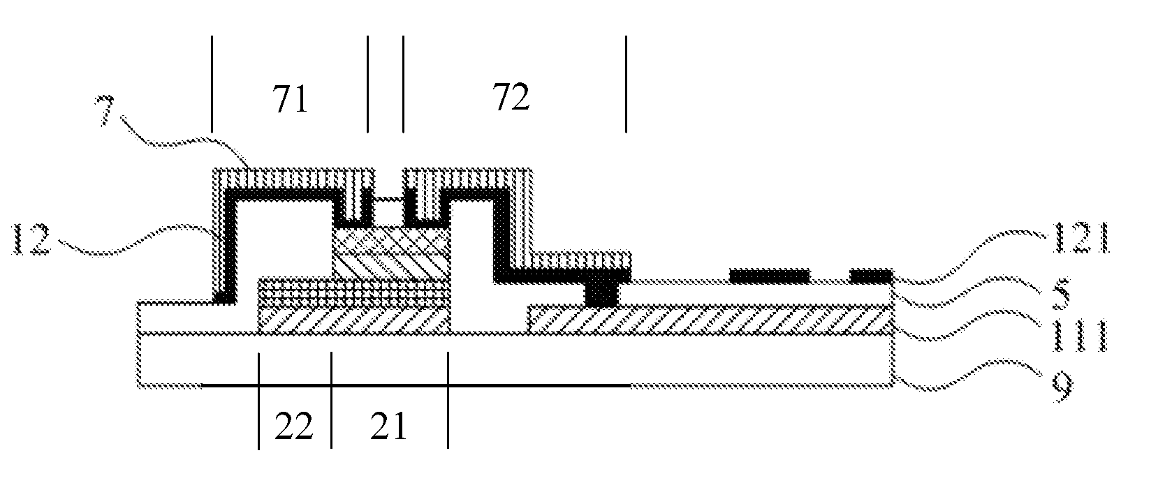
[0109]As shown in FIGS. 25 and 26, this embodiment provides an array substrate fabricated by the method described above, comprising a gate 21, a gate line 22, a gate insulation layer 31, a semiconductor layer 41, a first transparent electrode 111, a second transparent electrode 121, a source 71, a drain 72, and a passivation layer 5.

[0110]The passivation layer 5 covers the gate line 22, the gate 21, the gate insulation layer 31, the semiconductor layer 41 and the first transparent electrode 111.

[0111]The second transparent electrode 121 is provided above the passivation layer 5.

[0112]The source 71 and the drain 72 are provided above the passivation layer 5 and are electrically connected to the semiconductor layer 41 through a source via and a drain via provided in the passivation layer 5, respectively.

[0113]The gate 21 and the gate line 22 comprise a first transparent conductive material layer 11, the first transparent conductive material layer 11 is provided in the same layer as th...

third embodiment

[0120]This embodiment provides a liquid crystal display device comprising the array substrate described above. The liquid crystal display device may be applicable to liquid crystal display panels, electronic papers, cell phones, tablet computers, TV, displays, laptops, digital photo frames, navigation systems and any other product or component that has a display function.

[0121]The liquid crystal display device of the embodiment comprises the array substrate described above, and has advantages of simple fabricating method, good driving effect and high light transmittance.


PUM

PropertyMeasurementUnit
transparentaaaaaaaaaa
transparent conductiveaaaaaaaaaa
transmittanceaaaaaaaaaa

Abstract

An array substrate, a method of fabricating the same, and a liquid crystal display device are disclosed. The method comprises: sequentially forming a first transparent conductive material layer, an insulation material layer, a semiconductor material layer and a photoresist layer on a substrate base and forming patterns including a gate line, a gate, a gate insulation layer, a semiconductor layer and a first transparent electrode by patterning process; forming a passivation layer and forming a source via and a drain via connected to the semiconductor layer in the passivation layer; sequentially forming a second transparent conductive material layer and a source-drain metal layer and forming patterns including a source, a drain and a second transparent electrode by patterning process, the gate insulation layer is formed only on the gate and the gate line, the source and the drain include stacked second transparent conductive material layer and source-drain metal layer.

Description

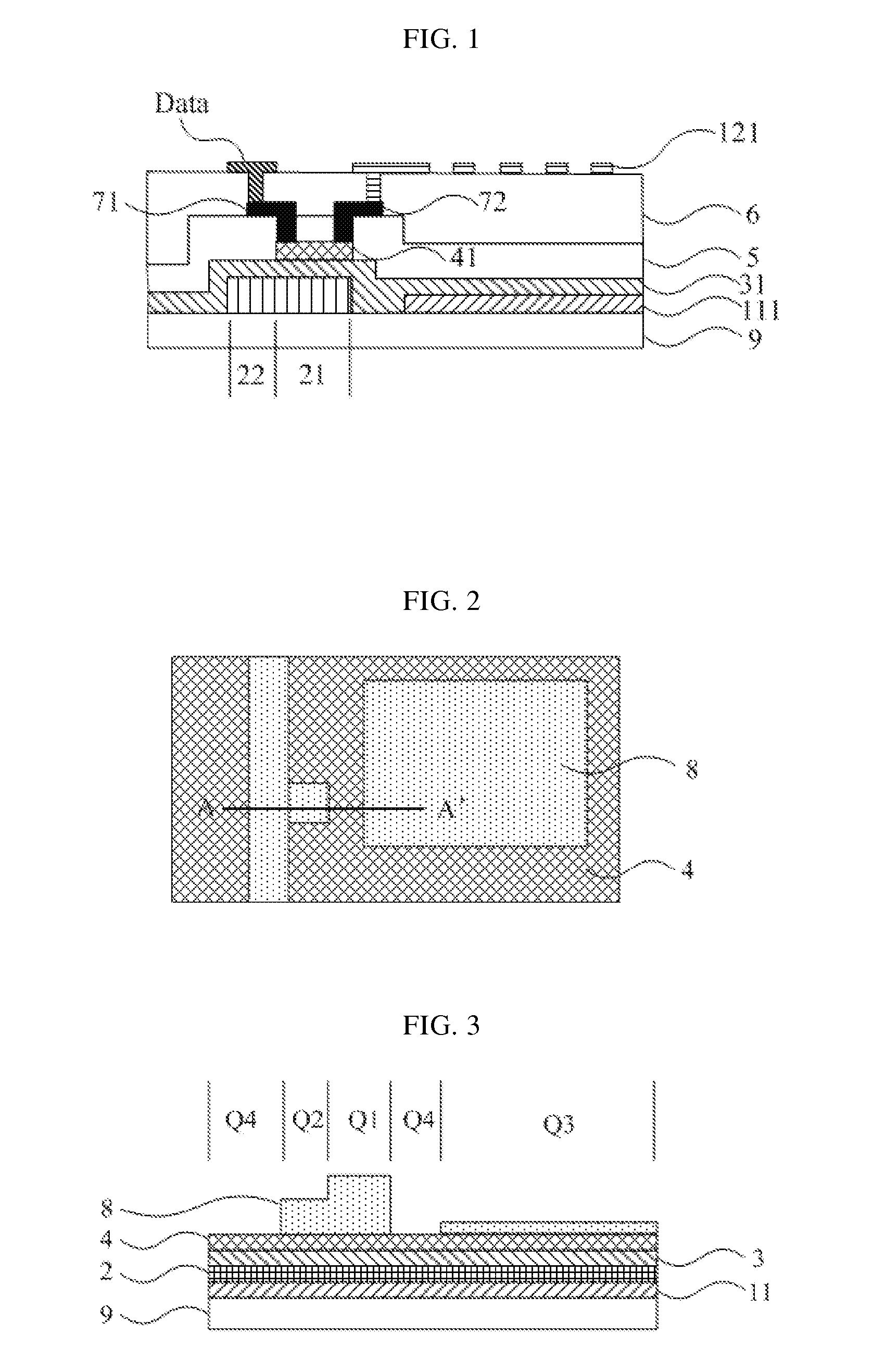
FIELD OF THE INVENTION[0001]The present invention relates to the field of liquid crystal display technology, and more particularly, to an array substrate, a method of fabricating the array substrate, and a liquid crystal display device.BACKGROUND OF THE INVENTION[0002]A liquid crystal display device of ADS mode (Advanced Super Dimension Switch mode) has advantages of wide viewing angle, high transmittance and high definition, thus the ADS mode becomes an important mode of the liquid crystal display device.[0003]As shown in FIG. 1, in an array substrate of the ADS mode, a first transparent electrode 111 of plate-shape, a gate 21 and a gate line 22 of a thin film transistor are provided on a substrate base 9, and a gate insulation layer 31 covers the first transparent electrode 111, the gate 21 and the gate line 22. A semiconductor layer 41 is provided above the gate 21, the semiconductor layer 41, an ohmic contact layer and a transition layer constitute an active region of the thin f...

Claims


Application Information

Patent Timeline
Patent Type & Authority Applications(United States)
IPC IPC(8): H01L27/12G02F1/1343G02F1/1362G02F1/1368H01L23/31H01L23/522H01L29/24H01L29/786
CPCH01L27/1225G02F1/136286G02F1/1368G02F1/13439H01L23/3171H01L29/7869H01L27/124H01L29/24H01L23/5226G02F1/136227H01L27/1259H01L27/1288H01L2224/24H01L2224/73267H01L2224/92244H01L2224/82G02F1/134372H01L21/77H01L27/127H01L2224/18
Inventor YOO, SEONGYEOLSONG, YOUNGSUKKIM, HEECHEOLCHOI, SEUNGJIN
Owner BOE TECH GRP CO LTD
Learn More