Method of generating clock and semiconductor device

Active Publication Date: 2015-10-01
LAPIS SEMICON CO LTD
View PDF10 Cites 7 Cited by
  • Summary
  • Abstract
  • Description
  • Claims
  • Application Information

AI Technical Summary

Benefits of technology

The present invention provides a method and device for generating a clock that are cost-effective and power-efficient. Additionally, the invention minimizes variations in data rate and temporal fluctuations.

Problems solved by technology

If it's the case, when the data rate deviation is large, it may not be able to meet the standard specification.
However, when the frequency of the master clock is adjusted, the master clock no longer has a common frequency.
Accordingly, it is difficult to reduce a cost of the master clock source (for example, a cost of an oscillation element), thereby increasing a cost of the communication system.
However, when the PLL is used, it is difficult to reduce power consumption of the communication system.
However, individual clock wave forms still include pluses with a long time span and pluses with a short time span.

Method used


Image

  • Method of generating clock and semiconductor device
  • Method of generating clock and semiconductor device
  • Method of generating clock and semiconductor device

Examples


Embodiment Construction

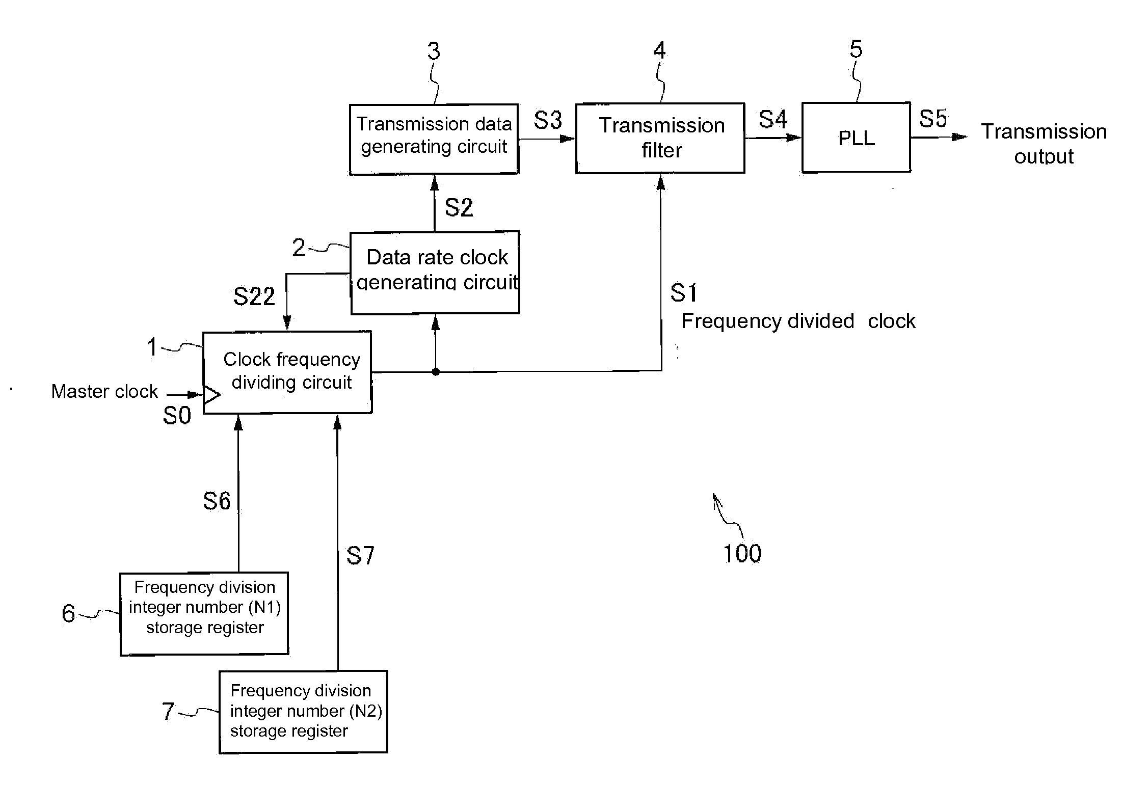
[0034]Hereunder, preferred embodiments of the present invention will be explained with reference to the accompanying drawings. First, a basic concept of the present invention will be explained.

[0035]In the embodiment, a method of generating a clock and a semiconductor device according to the present invention are applied to a transmission circuit using an FSK (Frequency Shift Keying) in a wireless communication system. Further, in the embodiment, a data rate is being oversampled.

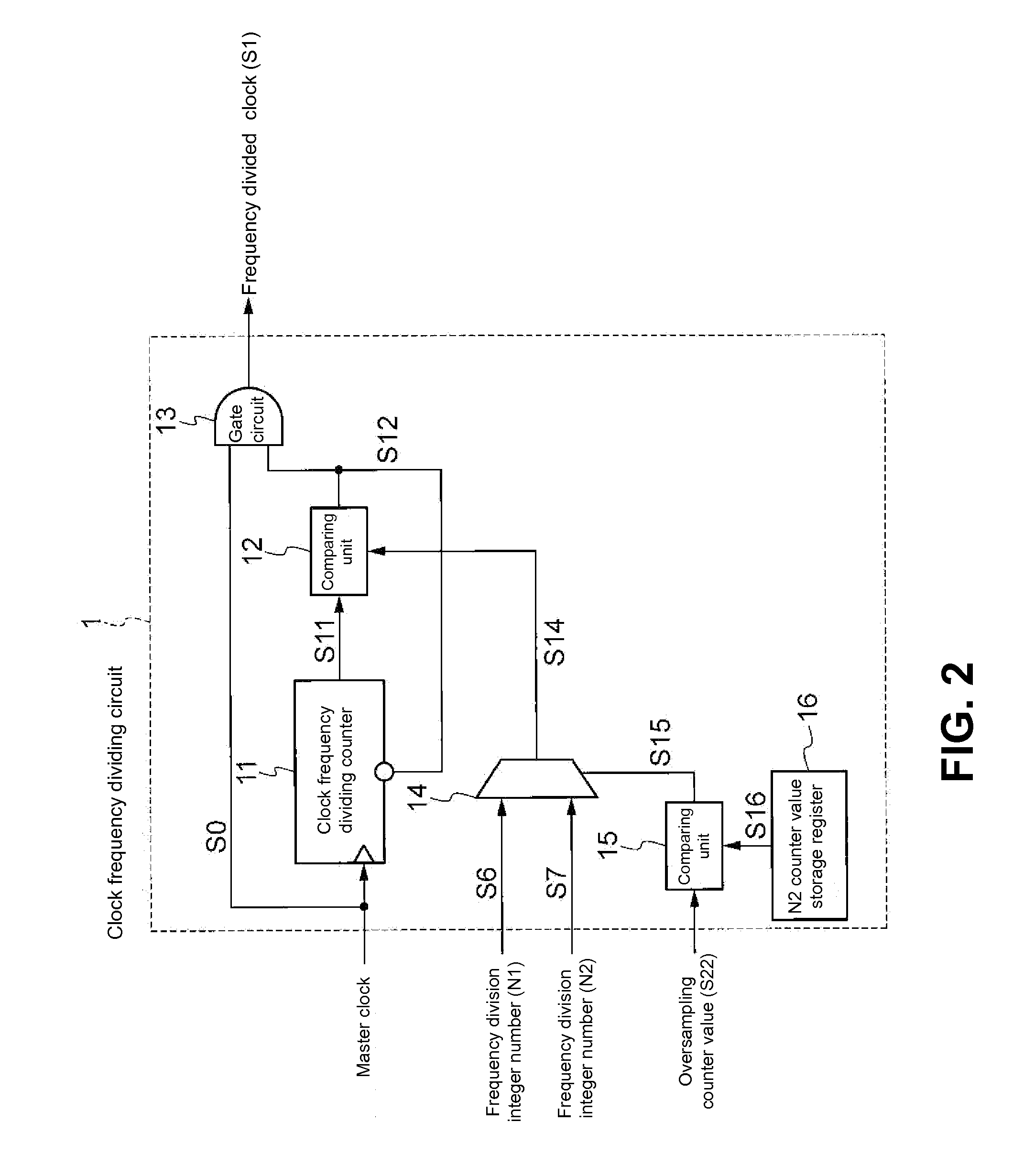
[0036]In the embodiment, the method of generating the clock and the semiconductor device according to the present invention are capable of generating a data rate clock obtained through dividing a frequency of a master clock using two frequency division integer numbers, i.e., a frequency division integer number N1 and a frequency division integer number N2. It should be noted that the frequency division integer number N1 is a frequency division integer number calculated with a conventional method, and the fre...


PUM


Abstract

A method of generating a clock includes the steps of calculating a first frequency division number through dividing a frequency of an input clock by a target frequency and a specific integer k (k≧2); calculating a second frequency division number according to the first frequency division number; dividing a period of time of one cycle of the target frequency by the specific integer k to obtain sections in a number of the specific integer k; dividing the frequency of the input clock with the second frequency division number within one of the sections; dividing the frequency of the input clock with the second frequency division number within each remaining one of the sections in a number of (k−1); and generating the clock having a frequency with one cycle equal to a period of time corresponding to each of the sections.

Description

BACKGROUND OF THE INVENTION AND RELATED ART STATEMENT[0001]The present invention relates to a method of generating a clock and a semiconductor device.[0002]In a communication system such as a wireless communication system, when a whole communication system is operated, a clock signal (a data rate clock) having a frequency is supplied to each component of the communication system according to a processing speed (a data rate) of a data signal of each component. Accordingly, in the communication system, it is necessary to generate the data rate clocks having various frequencies. To this end, the clock source is configured to generate a master clock having an accurately stabilized oscillation frequency, and the frequency of the master clock is divided to generate the data rate clocks having various frequencies, in consideration of simplification of a clock source of the data rate clock, synchronization of the whole communication system, and the like.[0003]As an example of a conventional...

Claims


Application Information

Patent Timeline
IPC IPC(8): H04L7/027H04L7/033
CPCH04L7/0334H04L7/027G06F1/04H03K21/023H03K23/42H03L7/081H03L7/18
Inventor HAFUKA, TAKAMITSU
Owner LAPIS SEMICON CO LTD
Why Eureka
Try Eureka