Structure mounted with electronic component
a technology of electronic components and structures, applied in the direction of fixed capacitor details, printed circuit non-printed electric components association, final product manufacture, etc., can solve the problems of limiting the increase in positioning accuracy between the respective components, affecting the quality of electronic components, so as to reduce or prevent the generation of defective mounting. , the degree of mounting position accuracy is high, and the joint strength is sufficient
- Summary
- Abstract
- Description
- Claims
- Application Information
AI Technical Summary
Benefits of technology
Problems solved by technology
Method used
Image
Examples
embodiment 1
Preferred Embodiment 1
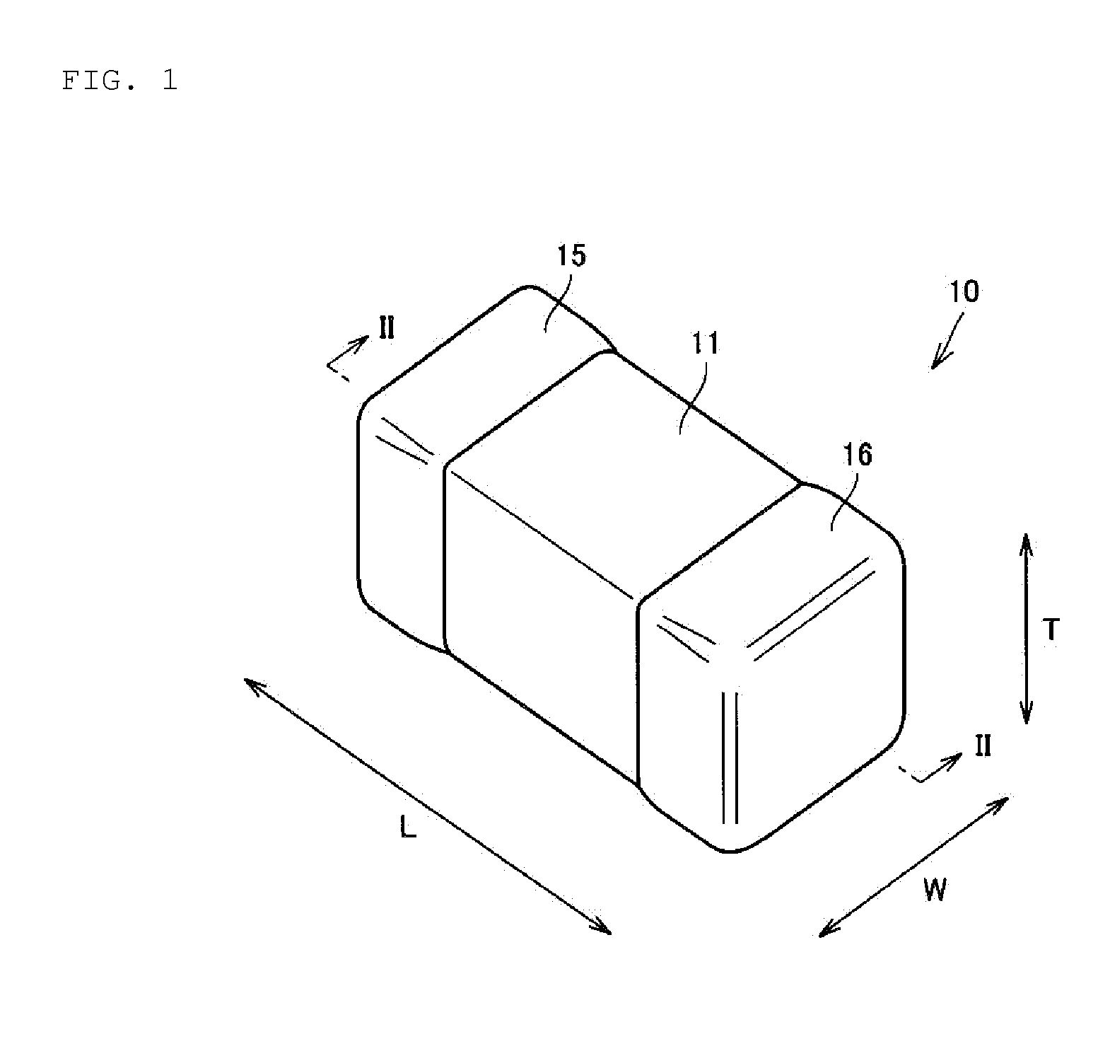
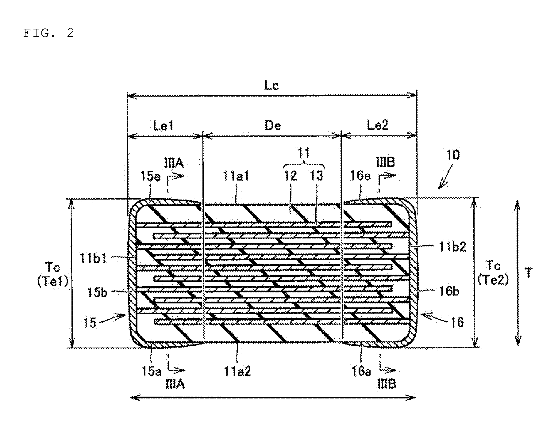
[0049]FIG. 1 is a perspective view of a laminated ceramic capacitor provided for a mounted structure in accordance with Preferred Embodiment 1 of the present invention. In addition, FIG. 2 is a schematic cross-sectional view along the line II-II shown in FIG. 1, and FIGS. 3A and 3B are schematic cross-sectional views along the line IIIA-IIIA and line IIIB-IIIB shown in FIG. 2. First, a laminated ceramic capacitor 10 provided for the mounted structure in accordance with the present preferred embodiment will be described with reference to FIGS. 1 to 3.
[0050]As shown in FIGS. 1 to 3, the laminated ceramic capacitor 10 is an electronic component which preferably has a generally rectangular or substantially rectangular parallelepiped shape, and includes a body 11, and a first external electrode 15 and a second external electrode 16 as a pair of external electrodes. It is to be noted that the rectangular or substantially rectangular parallelepiped shape also encompas...
embodiment 2
Preferred Embodiment 2
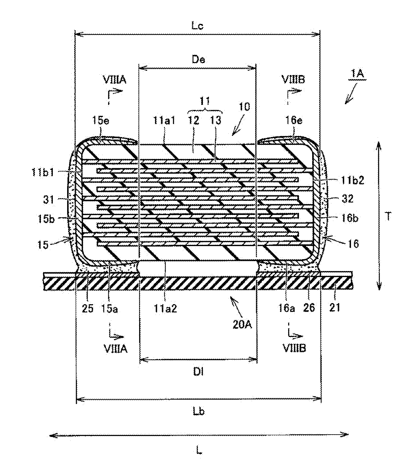
[0139]FIG. 17 is a schematic perspective view of a wiring substrate provided for a mounted structure according to the present preferred embodiment. In addition, FIG. 18 is a schematic cross-sectional view along the line XVIII-XVIII shown in FIG. 17, and FIGS. 19A and 19B are schematic cross-sectional views along the line XIXA-XIXA and line XIXB-XIXB shown in FIG. 18. Next, the wiring substrate 20B provided for the mounted structure according to the present preferred embodiment will be described with reference to FIG. 17 to FIGS. 19A and 19B.
[0140]As shown in FIGS. 17 to 18, the wiring substrate 20B, which has a generally plate-shaped configuration, is provided with a base 21, a solder resist 22, and conductive patterns 23.
[0141]The base 21 preferably is a plate-shaped and includes a pair of principal surfaces, and the solder resist 22 and conductive patterns 23 mentioned above are provided on at least one of the principal surfaces. As the material of the base 2...
PUM
| Property | Measurement | Unit |
|---|---|---|
| melting temperature | aaaaa | aaaaa |
| melting temperature | aaaaa | aaaaa |
| melting temperature | aaaaa | aaaaa |
Abstract
Description
Claims
Application Information
 - R&D
- Intellectual Property
- Life Sciences
- Materials
- Tech Scout
- Unparalleled Data Quality
- Higher Quality Content
- 60% Fewer Hallucinations
Browse by: Latest US Patents, China's latest patents, Technical Efficacy Thesaurus, Application Domain, Technology Topic, Popular Technical Reports.
© 2025 PatSnap. All rights reserved.Legal|Privacy policy|Modern Slavery Act Transparency Statement|Sitemap|About US| Contact US: help@patsnap.com


