Transistor having dual work function buried gate electrode and method for fabricating the same

a dual work function, gate electrode technology, applied in the field of transistors, can solve the problems of increasing gate resistance, causing probable causes, and causing gate-induced drain leakage (gidl), and achieve the effect of reducing gate-induced drain leakage and improving current drivability

Active Publication Date: 2015-07-30
SK HYNIX INC
View PDF7 Cites 37 Cited by
  • Summary
  • Abstract
  • Description
  • Claims
  • Application Information

AI Technical Summary

Benefits of technology

[0010]Various embodiments of the present invention are directed to a buried gate type transistor and a method for fabricating the same, for reducing gate-induced drain leakage and improving current drivability.

Problems solved by technology

However, a concern is likely to be caused due to the high work function, since gate-induced drain leakage (GIDL) increases where the metal gate electrode and junction regions overlap, in the source / drain regions.
Particularly, in a buried gate type transistor, since the overlap area between a buried metal gate electrode and source / drain regions is large, gate-induced drain leakage (GIDL) may be an issue.
Nevertheless, if the height of the buried metal gate electrode is lowered, there is a concern that gate resistance increases and the current drivability of the transistor is degraded.

Method used


Image

  • Transistor having dual work function buried gate electrode and method for fabricating the same
  • Transistor having dual work function buried gate electrode and method for fabricating the same
  • Transistor having dual work function buried gate electrode and method for fabricating the same

Examples


first embodiment

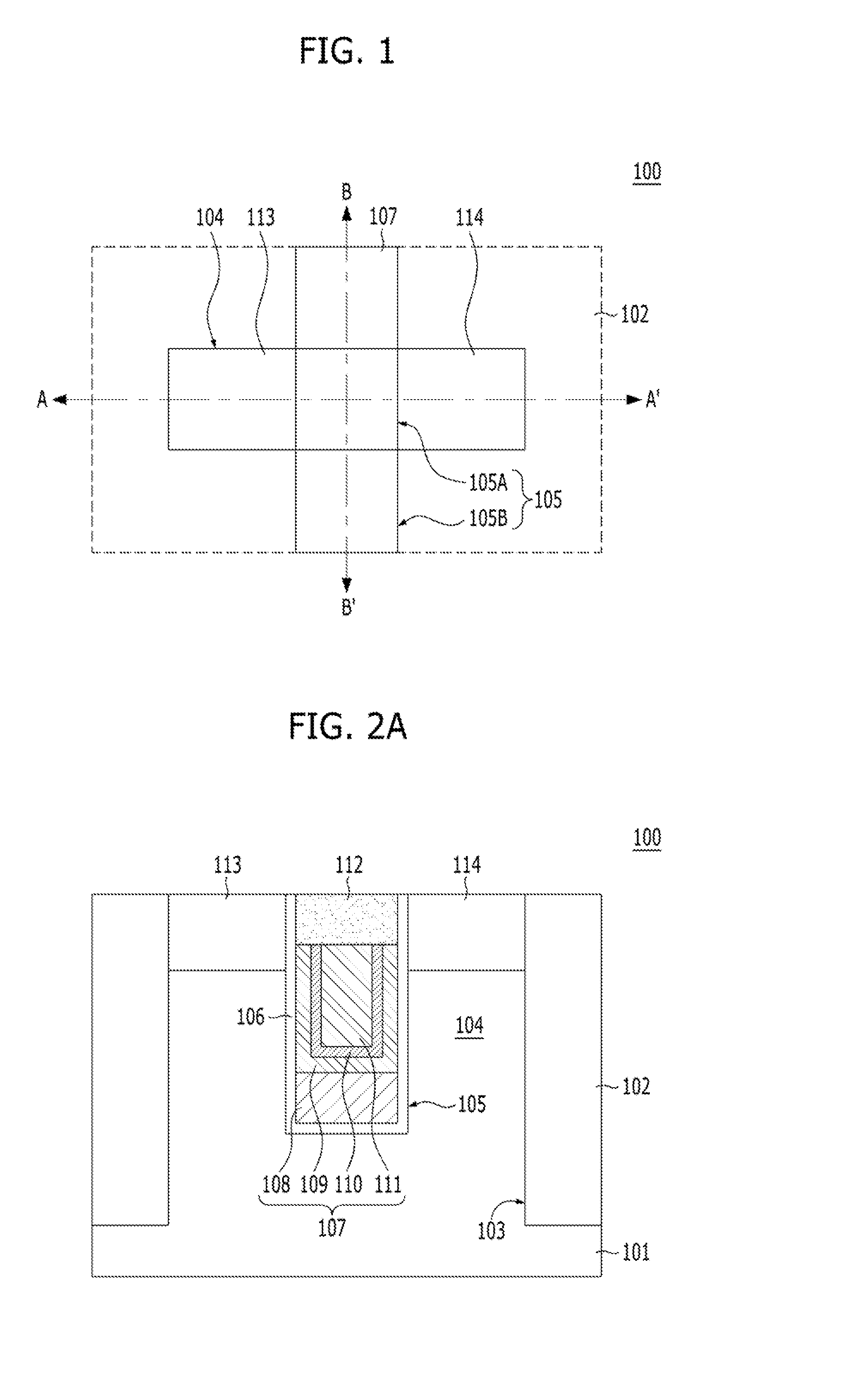
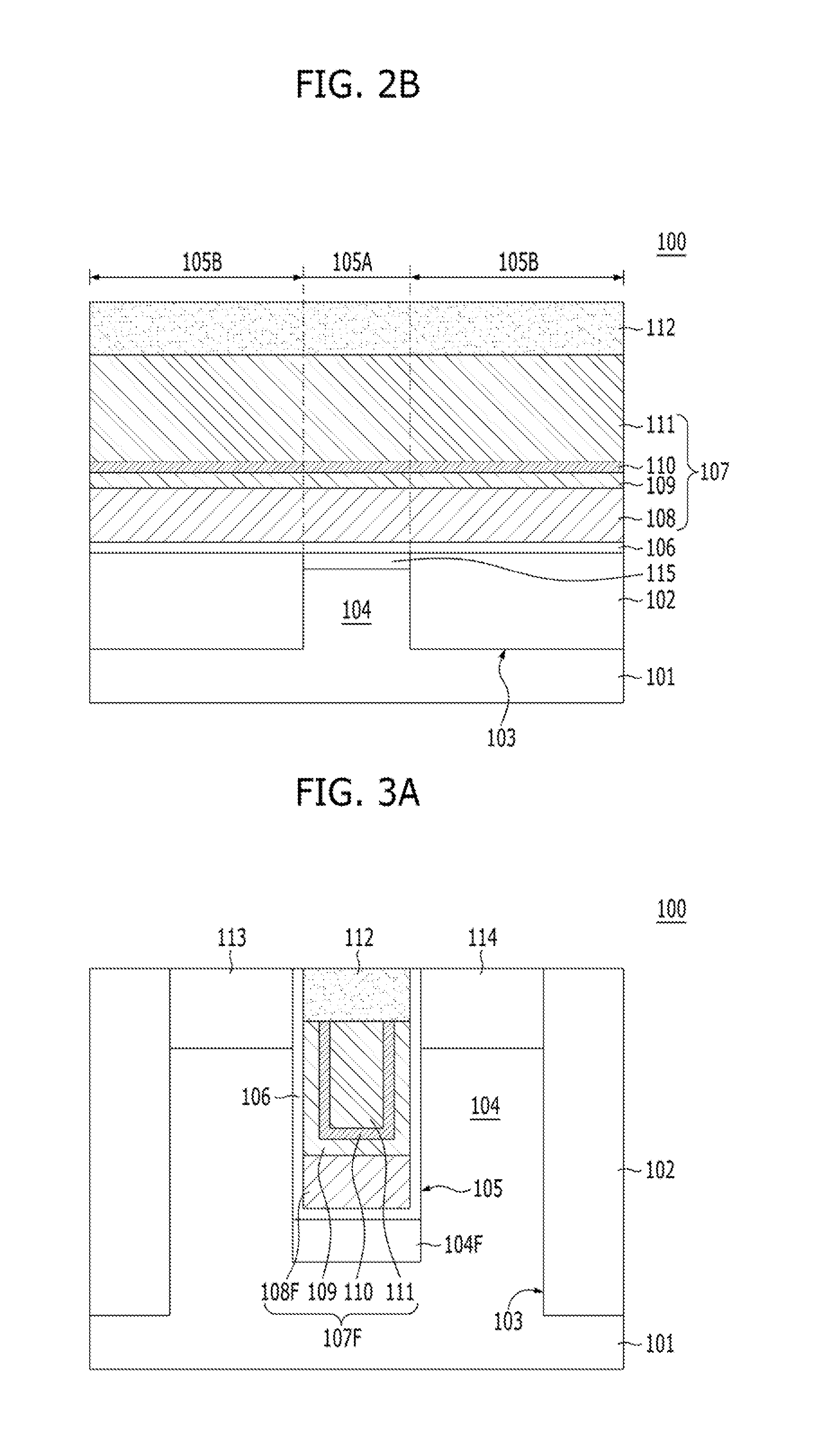
[0033]FIG. 1 is a plan view illustrating a transistor in accordance with the present invention. FIG. 2A is a cross-sectional view taken along the line A-A′ of FIG. 1. FIG. 2B is a cross-sectional view taken along the line B-B′ of FIG. 1.

[0034]A transistor 100 will be described with reference to FIGS. 1, 2A and 2B.

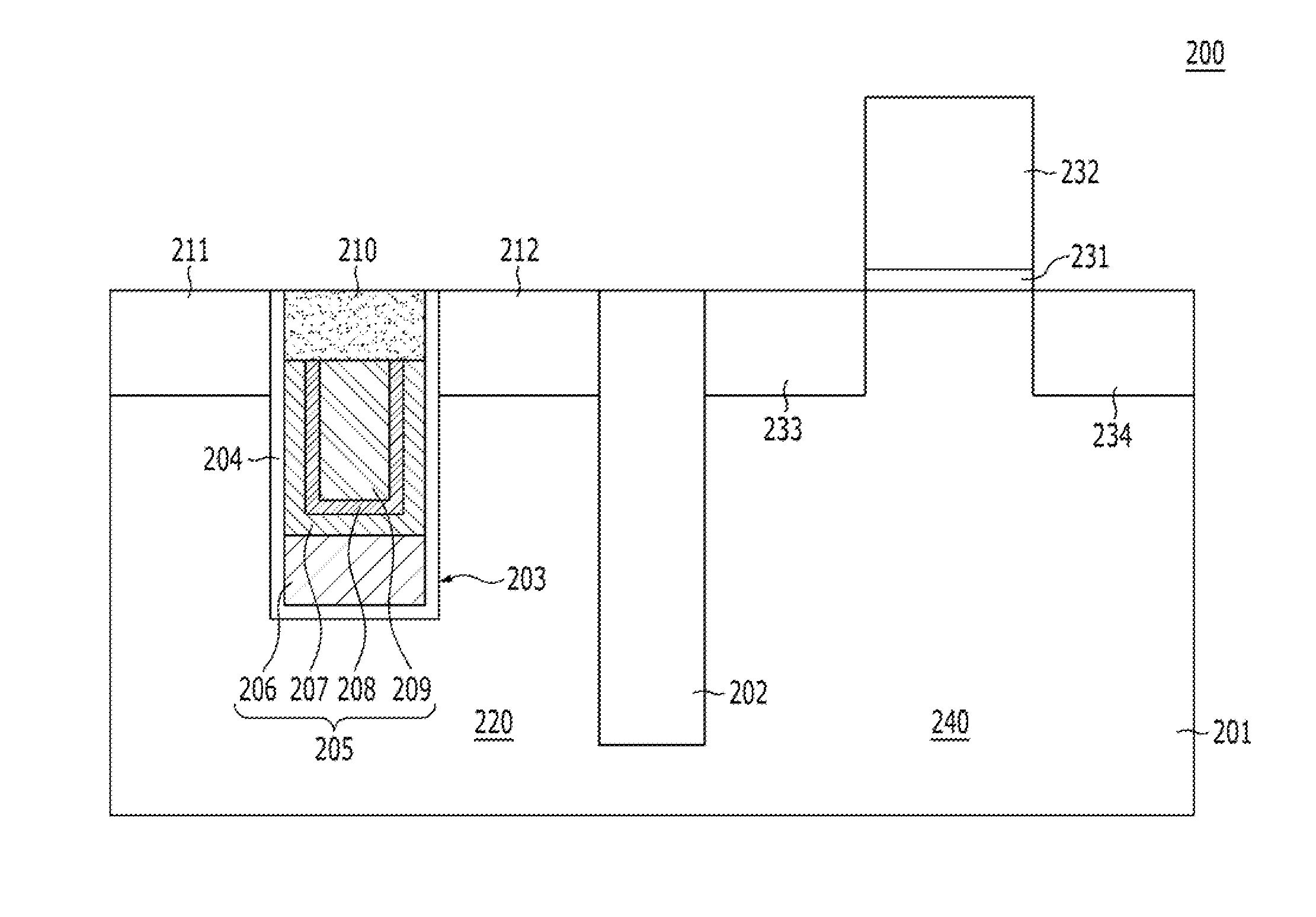
[0035]A substrate 101 is prepared. The substrate 101 may include a semiconductor substrate. The substrate 101 may be a silicon substrate. An isolation layer 102 is formed in the substrate 101. The isolation layer 102 may include an isolation dielectric layer which is gapfilled in an isolation trench 103. An active region 104 is defined in the substrate 101 by the isolation layer 102.

[0036]A trench 105 which has a predetermined depth is defined in the substrate 101. The trench 105 may be a line type which extends in any one direction. The trench 105 has a shape which extends across the active region 104 and the isolation layer 102. The trench 105 has a depth that is shallowe...

second embodiment

[0049]The transistor 100 in accordance with the present invention is referred to as a buried gate type fin channel transistor.

[0050]According to the first embodiment and the second embodiment, the low resistance of the buried gate electrodes 107 shown in FIG. 2B, and 107F is secured by the second electrode 111. Channel dose may be decreased by the first electrodes 108 and 108F. Gate-induced drain leakage (GIDL) may be reduced by the liner electrode 109. An abnormal reaction between the liner electrode 109 and the second electrode 111 may be prevented by the barrier layer 110.

[0051]A method for fabricating the transistor in accordance with the first embodiment of the present invention will now be described. FIGS. 4A to 4F are views illustrating an exemplary method for fabricating the transistor in accordance with the first embodiment of the present invention. FIGS. 4A to 4F are cross-sectional views take along the line A-A′ of FIG. 1.

[0052]As shown in FIG. 4A, an isolation layer 12 i...


PUM

PropertyMeasurementUnit
work functionaaaaaaaaaa
mid-gap work functionaaaaaaaaaa

Abstract

A transistor having a source region and a drain region which are separately formed in a substrate, a trench which is defined in the substrate between the source region and the drain region, and a gate electrode which is formed in the trench. The gate electrode includes a first electrode buried over a bottom of the trench; a second electrode formed over the first electrode; and a liner electrode having an interface part which is positioned between the first electrode and the second electrode and a side part, which is positioned on sidewalls of the second electrode and overlaps with the source region and the drain region.

Description

CROSS-REFERENCE TO RELATED APPLICATIONS[0001]The present application claims priority of Korean Patent. Application No. 10-2014-0011584, filed on Jan. 29, 2014, which is incorporated herein by reference in its entirety.BACKGROUND[0002]1. Field[0003]Exemplary embodiments of the present invention relate to a transistor, and more particularly, to a transistor having a dual work function buried gate electrode and a method for fabricating the same.[0004]2. Description of the Related Art[0005]A metal gate electrode may be applied as the gate electrode of a transistor. Gate resistance may be decreased by a metal gate electrode that has a low resistance. Additionally, since the metal gate electrode may have a high work function, the channel dose may be decreased resulting in a reduction of leakage current and improved transistor performance.[0006]However, a concern is likely to be caused due to the high work function, since gate-induced drain leakage (GIDL) increases where the metal gate ele...

Claims


Application Information

Patent Timeline
Patent Type & Authority Applications(United States)
IPC IPC(8): H01L29/423H01L21/28H01L29/66H01L29/78H01L27/24H01L27/108
CPCH01L29/4236H01L27/2454H01L21/28008H01L29/66666H01L29/7827H01L27/108H01L29/4983H10B63/30H10B61/22H10N70/231H10N70/826H10N70/882H10N70/8833H10B12/053H10B12/482H01L29/66795H01L29/785H01L21/762
Inventor OH, TAE-KYUNGKIM, SU-HOLEE, JIN-YUL
Owner SK HYNIX INC
Why Eureka
Try Eureka