
Carrier-bonding methods and articles for semiconductor and interposer processing

a carrier and interposer technology, applied in semiconductor devices, semiconductor/solid-state device details, electrical devices, etc., can solve the problems of carrier not providing sufficient support to prevent warping, wafers becoming even more fragile and susceptible to damage, and reducing so as to reduce the need for back-end thinning and easy separation

Active Publication Date: 2015-04-16
CORNING INC
View PDF5 Cites 38 Cited by
  • Summary
  • Abstract
  • Description
  • Claims
  • Application Information

AI Technical Summary

Benefits of technology

The patent text describes an improved carrier-substrate solution for use in the processing of thin wafers, which can withstand high temperatures and provide easy debonding after processing. This solution allows for the use of thinner wafers and reduces the need for back-end thinning, thereby improving yield and reducing costs. The use of carrier-supported wafers also allows for easy testing and screening of wafers before device processing, leading to improved yields. The patent also describes the use of interposers made of polysilicon, single crystal silicon, or glass to improve communication speeds and the lead application of this technology in the manufacturing of field programmable gate arrays (FPGA). The bonding solutions described in the patent have been developed and tested with high yield and low processing times, using thin form at final thicknesses for glass and silicon wafers.

Problems solved by technology

This process of thinning the wafer can damage the edges of the wafer and can make the wafer even more fragile and susceptible to damage during subsequent transportation and processing of the wafer.
It has been found, however, that the wafer may warp during processing and that the typical carrier does not provide sufficient support to prevent warping.
As a result of the warpage of the wafer, processes may fail and / or cause alarm conditions.
Due to some of the high temperature (e.g., ≧500° C., in some instances, 500° C. to 650° C., and in some cases up to 700° C.) processes associated with FEOL processing, many adhesive based solutions cannot be used, as they may fail to hold the bond, they may outgas contaminants, or both.
Moreover, most temporary adhesives have high CTEs which are mismatched with the wafer and carrier materials, and are difficult to remove while leaving the delicate microstructures on the wafer intact.
Additionally, the CTE mismatch between the adhesive and the wafer and / or carrier materials may cause undesirable warping of the wafer.
Still further, adhesive may find its way into the vias of an interposer when bonding to a carrier and undesirably prevent metallization of at least part of the via.
Interposers are by definition thin, as thick interposers cause an unacceptable form factor (height) and performance (heat) obstacles.
Again, substrates of these thicknesses generally cannot be processed in existing tools.
The attractiveness of glass is performance and cost, but no solution has yet existed today to realize these advantages for glass.

Method used


Image

  • Carrier-bonding methods and articles for semiconductor and interposer processing
  • Carrier-bonding methods and articles for semiconductor and interposer processing
  • Carrier-bonding methods and articles for semiconductor and interposer processing

Examples


example 4a

[0148]A glass carrier with its bonding surface O2 plasma and SC1 treated was then treated with 1% dodecyltriethoxysilane (DDTS) in toluene, and annealed at 150° C. in vacuum for 1 hour to complete condensation. DDTS treated surfaces exhibit a surface energy of 45 mJ / m2. As shown in Table 4, a glass thin sheet (having been SC1 cleaned and heated at 400° C. in a vacuum for one hour) was bonded to the carrier bonding surface having the DDTS surface modification layer thereon. This article survived wet and vacuum process tests but did not survive thermal processes over 400° C. without bubbles forming under the carrier due to thermal decomposition of the silane. This thermal decomposition is expected for all linear alkoxy and chloro alkylsilanes R1xSi(OR2)y(Cl)z where x=1 to 3, and y+z=4-x except for methyl, dimethyl, and trimethyl silane (x=1 to 3, R1=CH3) which produce coatings of good thermal stability.

example 4b

[0149]A glass carrier with its bonding surface O2 plasma and SC1 treated was then treated with 1% 3,3,3, trifluoropropyltritheoxysilane (TFTS) in toluene, and annealed at 150° C. in vacuum for 1 hour to complete condensation. TFTS treated surfaces exhibit a surface energy of 47 mJ / m2. As shown in Table 4, a glass thin sheet (having been SC1 cleaned and then heated at 400° C. in a vacuum for one hour) was bonded to the carrier bonding surface having the TFTS surface modification layer thereon. This article survived the vacuum, SRD, and 400° C. process tests without permanent bonding of the glass thin sheet to the glass carrier. However, the 600° C. test produced bubbles forming under the carrier due to thermal decomposition of the silane. This was not unexpected because of the limited thermal stability of the propyl group. Although this sample failed the 600° C. test due to the bubbling, the material and heat treatment of this example may be used for some applications wherein bubbles...

example 4c

[0150]A glass carrier with its bonding surface O2 plasma and SC1 treated was then treated with 1% phenyltriethoxysilane (PTS) in toluene, and annealed at 200° C. in vacuum for 1 hour to complete condensation. PTS treated surfaces exhibit a surface energy of 54 mJ / m2. As shown in Table 4, a glass thin sheet (having been SC1 cleaned and then heated at 400° C. in a vacuum for one hour) was bonded to the carrier bonding surface having the PTS surface modification layer. This article survived the vacuum, SRD, and thermal processes up to 600° C. without permanent bonding of the glass thin sheet with the glass carrier.


PUM


Abstract

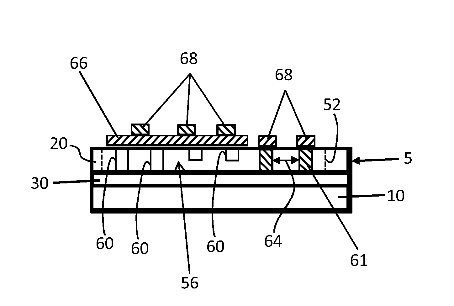
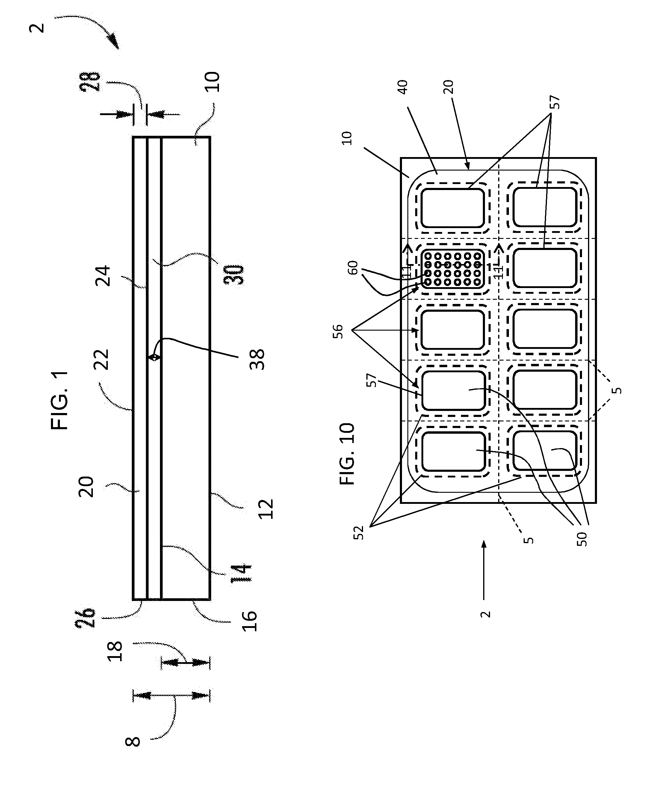
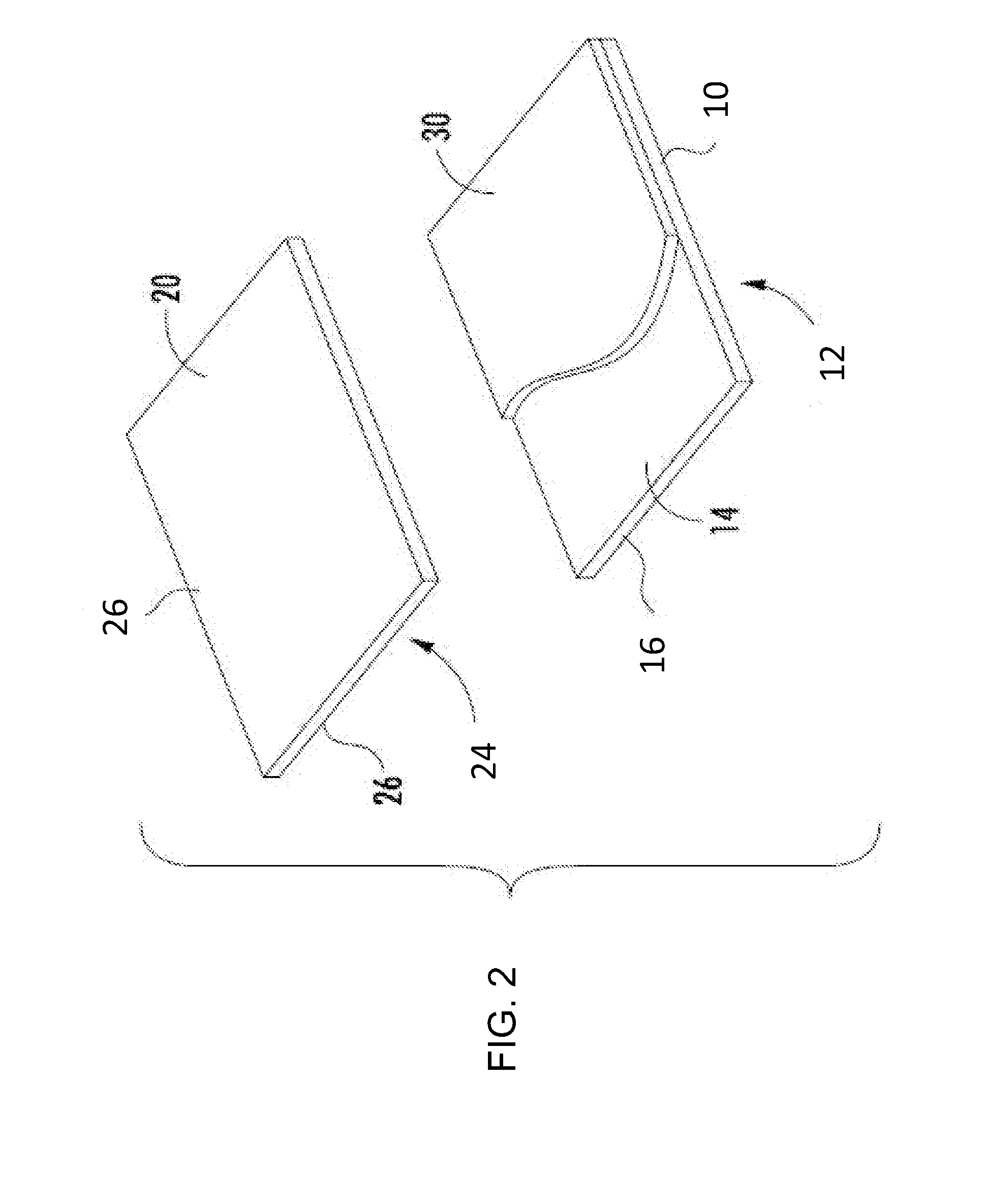
A thin sheet (20) disposed on a carrier (10) via a surface modification layer (30) to form an article (2), wherein the article may be subjected to high temperature processing, as in FEOL semiconductor processing, not outgas and have the thin sheet maintained on the carrier without separation therefrom during the processing, yet be separated therefrom upon room temperature peeling force that leaves the thinner one of the thin sheet and carrier intact. Interposers (56) having arrays (50) of vias (60) may be formed on the thin sheet, and devices (66) formed on the interposers. Alternatively, the thin sheet may be a substrate on which semiconductor circuits are formed during FEOL processing.

Description

[0001]This application claims the benefit of priority of U.S. Provisional Application Ser. No. 61 / 890,524, filed on Oct. 14, 2013, the content of which is relied upon and incorporated herein by reference in its entirety.BACKGROUND[0002]1. Field of the Invention[0003]The present invention is generally directed to carriers bonded to and removed from thinner substrates to allow processing of the thinner substrates. More particularly, the present invention is directed to methods and apparatuses for bonding wafers to carriers for semiconductor and / or interposer processing, and then debonding the wafers from the carriers after such processing.[0004]2. Technical Background[0005]Semiconductor devices are fabricated by forming active devices on or within a semiconductor wafer. The semiconductor wafer may comprise, for example, glass, silicon, polysilicon, single crystal silicon, silicon oxide, aluminum oxide, combinations of these, and / or the like. Hundreds or thousands of integrated circuit...

Claims


Application Information

Patent Timeline
IPC IPC(8): H01L21/683H01L23/00H01L23/498
CPCH01L21/6835H01L23/49827H01L24/83H01L24/94H01L2224/83052H01L2224/8385H01L2924/201H01L2924/2011H01L2924/10253H01L2924/05432H01L2924/05442H01L2924/20641H01L2924/20642H01L2924/20107H01L2924/1461H01L2924/1432H01L2924/12041H01L2924/12H01L2924/10271H01L2924/10329H01L2924/1033H01L2924/01029H01L2924/2064H01L2221/68318H01L2221/68327H01L2221/68331H01L2221/68345H01L2221/68381H01L2924/15788H01L21/486H01L23/15H01L2924/00
Inventor ENICKS, DARWIN GENEKEECH, JOHN TYLERSHOREY, ARIC BRUCETHOMAS, III, WINDSOR PIPES
Owner CORNING INC
Learn More