Cost Effective Method of Forming Embedded DRAM Capacitor

a capacitor and dram technology, applied in capacitors, semiconductor devices, semiconductor/solid-state device details, etc., can solve the problems of difficult optimization of the thickness parameter of such high-k dielectric films, limited height of such cylindrical capacitors, and ineffective limitation of loading effects

Active Publication Date: 2015-04-16
MOSAID TECH
View PDF1 Cites 38 Cited by
  • Summary
  • Abstract
  • Description
  • Claims
  • Application Information

AI Technical Summary

Problems solved by technology

While thinner dielectric films can be made using a high-k dielectric material having a high dielectric constant k, the thickness parameter of such high-k dielectric films is difficult to optimize as technological generations progress.
While plate overlap can be increased by forming large, overlapping lateral capacitor plate layers, such structures reduce the pattern density at the memory region, resulting in loading effects during photo lithography, etch, and polishing steps.
However, the height of such cylindrical capacitors is effectively limited by the constraints from high aspect ratio contact etch limitations which prevent contact etching from proceeding to a sufficient depth.
However, such metal interconnect capacitors are typically limited to the height of one metal level due to the blocking of barrier metal at the bottom of the metal interconnect, and also require expensive photo step and etching of high aspect ratio contacts for capacitors.

Method used


Image

  • Cost Effective Method of Forming Embedded DRAM Capacitor
  • Cost Effective Method of Forming Embedded DRAM Capacitor
  • Cost Effective Method of Forming Embedded DRAM Capacitor

Examples


Embodiment Construction

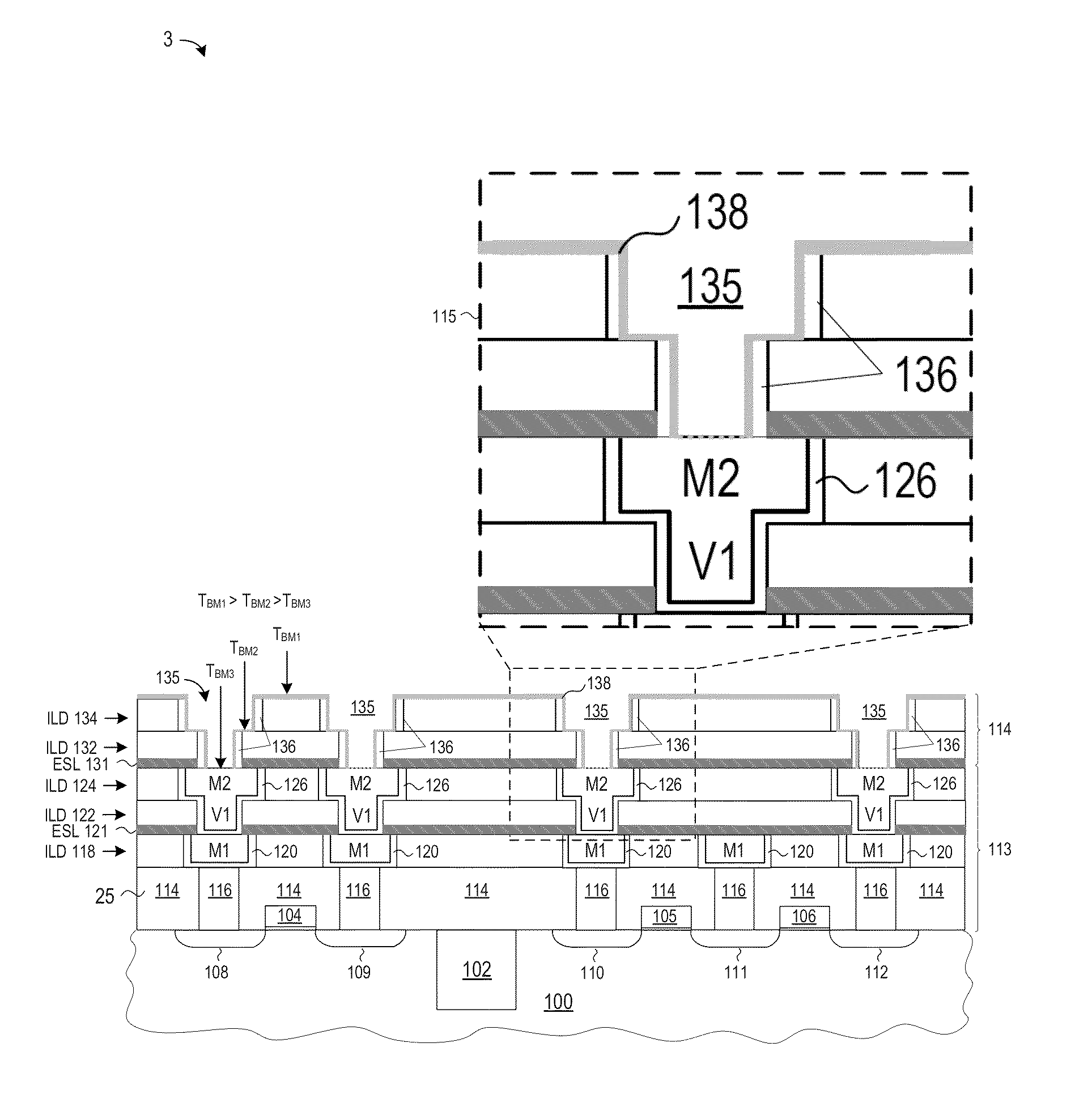
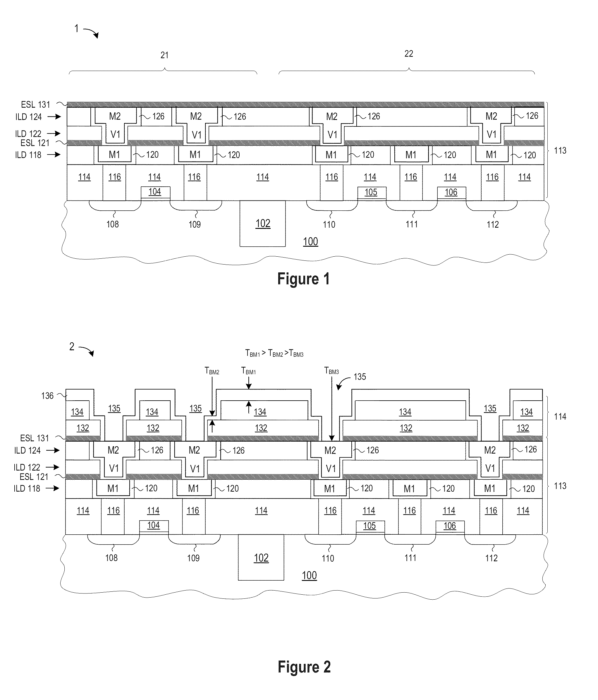
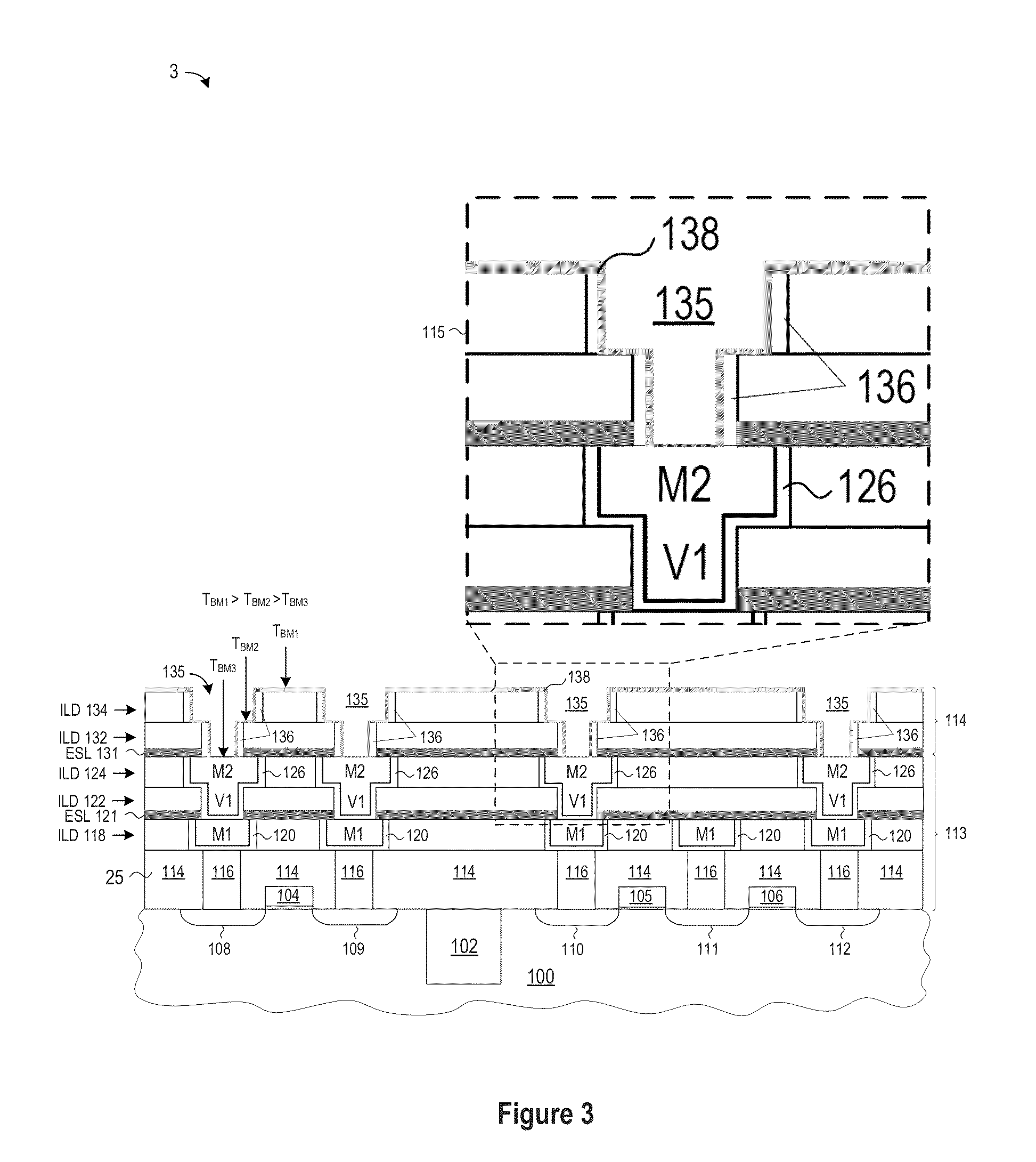
[0009]A high capacitance embedded metal interconnect capacitor and associated fabrication processes are disclosed in which a directional barrier metal formation sequence is used in a dual damascene copper process to form multi-layer stacked copper interconnect structures having a barrier metal sidewall layer on each via and trench with very little or no barrier metal layer remaining at the bottom of each via hole. In selected embodiments, the directional barrier metal formation sequence includes a first barrier metal layer that is conformally deposited or sputtered on the via and trench openings to a predetermined thickness. Subsequently, a second barrier metal layer is formed on the first barrier metal layer by sputtering with an applied bias to remove or substantially thin the barrier metal layers at the bottom of the trench and via hole. As a result, the dual damascene copper interconnect has very little or no barrier metal at the bottom of the via hole. By applying a selective e...


PUM

PropertyMeasurementUnit
thicknessesaaaaaaaaaa

Abstract

A high capacitance embedded metal interconnect capacitor and associated fabrication processes are disclosed for using a directional barrier metal formation sequence in a dual damascene copper process to form multi-layer stacked copper interconnect structure having reduced barrier metal layer formation at the bottom of each via hole so that the multi-layer stacked copper interconnect structure may be readily removed and replaced with high capacitance MIM capacitor layers.

Description

BACKGROUND OF THE INVENTION[0001]1. Field of the Invention[0002]The present invention is directed in general to integrated circuit devices and methods for manufacturing same. In one aspect, the present invention relates to formation of a capacitor with metal interconnect structures.[0003]2. Description of the Related Art[0004]Integrated circuit devices, such as dynamic random access memory (DRAM) devices, increasingly require high performance capacitors with sufficient capacitance to extend the refresh period and increase tolerance to alpha particles. For example, a typical DRAM cell configuration includes a capacitor for storing a charge (i.e., the bit of information) and an access transistor that provides access to the capacitor during read and write operations. To provide the required capacitance for such high performance cell capacitors, the overlap area between an upper electrode (plate electrode) and a lower electrode (storage node electrode) should be increased and / or the thi...

Claims


Application Information

Patent Timeline
Patent Type & Authority Applications(United States)
IPC IPC(8): H01L27/108H01L49/02H01L23/532
CPCH01L27/10844H01L23/53238H01L28/75H01L27/108H01L23/53295H01L28/87H01L28/91H01L2924/0002H01L23/5223H01L21/76844H01L21/76865H10B12/315H10B12/09H10B12/50H10B12/0335H01L2924/00H10B12/01H10B12/00
Inventor LEE, SOOGEUN
Owner MOSAID TECH
Why Eureka
Try Eureka