Controlling LED emission pattern using optically active materials
- Summary
- Abstract
- Description
- Claims
- Application Information
AI Technical Summary
Benefits of technology
Problems solved by technology
Method used
Image

Examples
Embodiment Construction
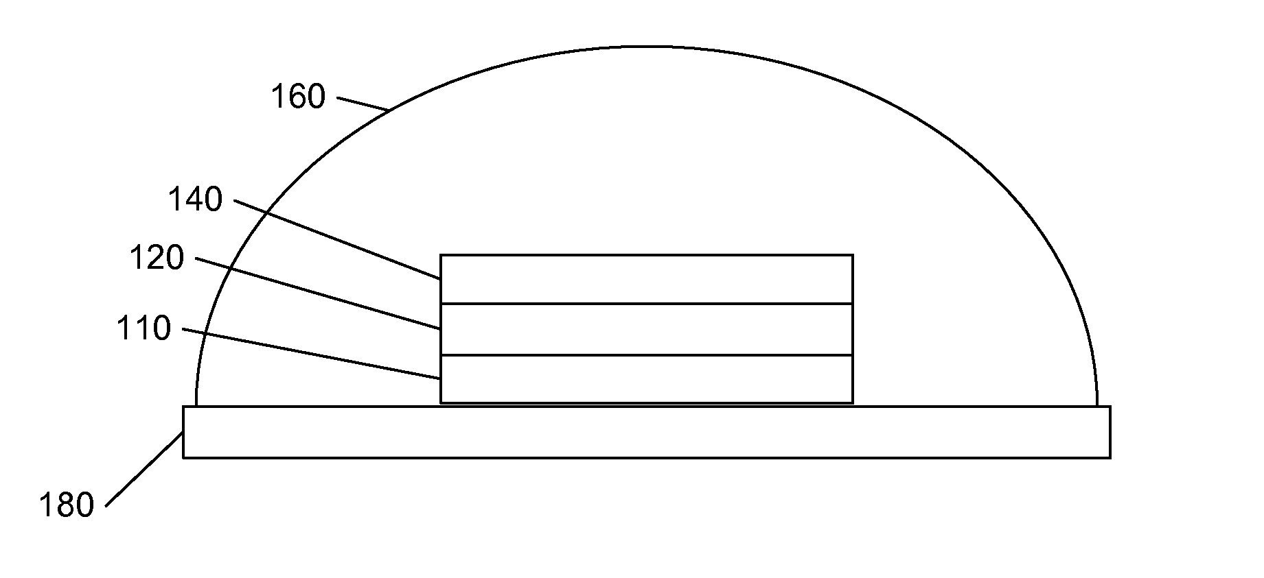
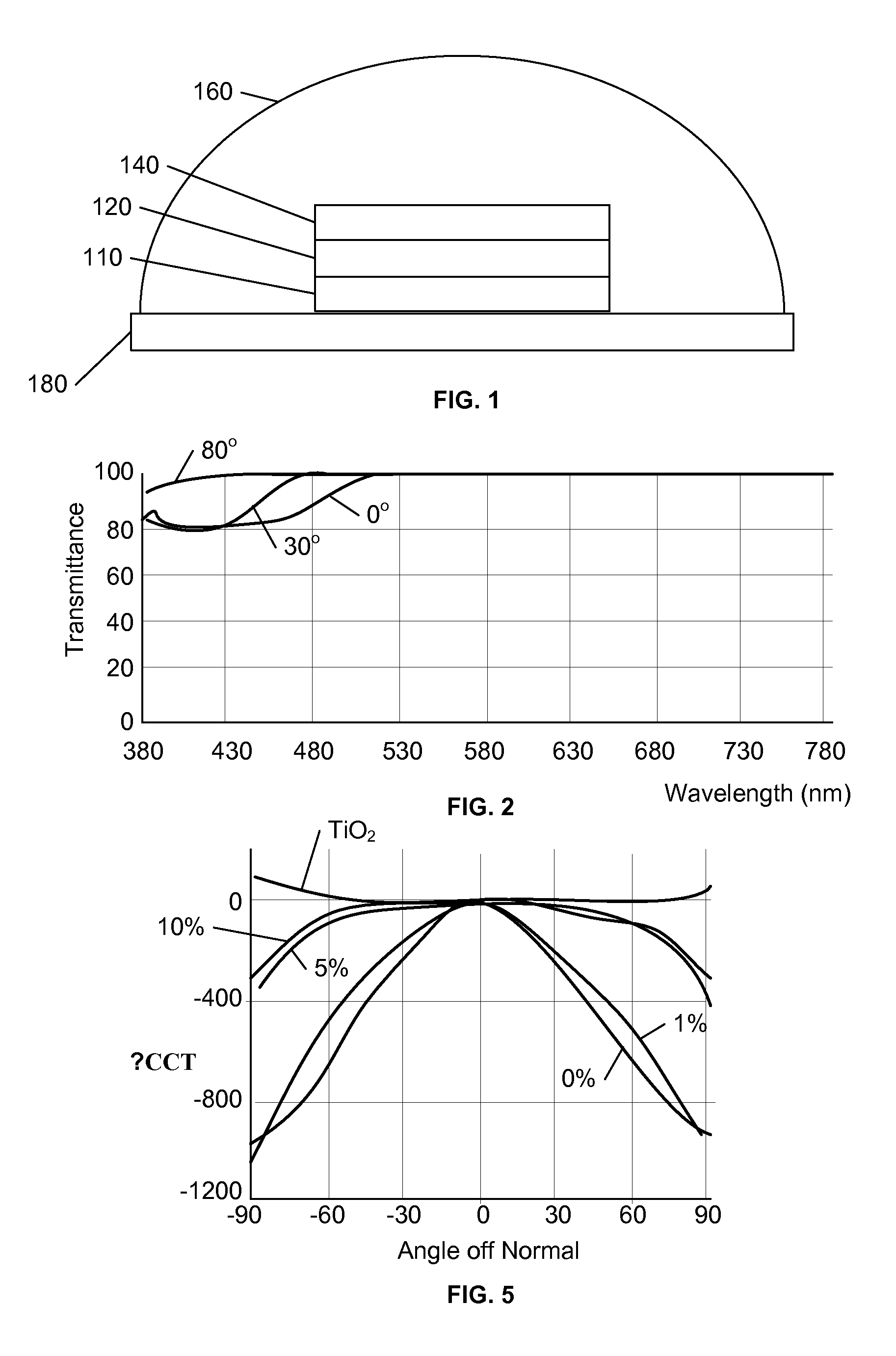
[0017]FIG. 1 shows a first embodiment of a light emission diode (LED) assembly according to the invention with a LED die 110, a wavelength conversion layer 120 and a filter layer 140. The led die 110, the wavelength conversion layer 120 and the filter 140 may be covered by a protective housing 160, which may be shaped to provide a particular light emission pattern.
[0018]The LED die 110 emits blue light with a wavelength of about 400 nm to 500 nm and is positioned on a substrate 180 of the LED assembly. On the top of the LED die 110 the wavelength conversion layer 120 is positioned.
[0019]The wavelength conversion layer 120 may, for example, emit yellow light with a wavelength of about 570 nm to 590 nm when illuminated by blue light. The wavelength conversion layer 120 may comprise a Lumiramic plate and / or a phosphor powder embedded in a transparent matrix material. The thickness of the wavelength conversion layer 120 may be about 100 μm to 120 μm. On the top of the wavelength convers...
PUM
 Abstract
Description
Claims
Application Information
 - R&D
- Intellectual Property
- Life Sciences
- Materials
- Tech Scout
- Unparalleled Data Quality
- Higher Quality Content
- 60% Fewer Hallucinations
Browse by: Latest US Patents, China's latest patents, Technical Efficacy Thesaurus, Application Domain, Technology Topic, Popular Technical Reports.
© 2025 PatSnap. All rights reserved.Legal|Privacy policy|Modern Slavery Act Transparency Statement|Sitemap|About US| Contact US: help@patsnap.com