Image Sensor and Manufacturing Method Thereof

a technology of image sensor and manufacturing method, which is applied in the field of semiconductor devices, can solve problems such as degrading the performance of image sensors, and achieve the effect of reducing the loss of voltage transmission

Inactive Publication Date: 2015-01-15
GALAXYCORE SHANGHAI
View PDF3 Cites 0 Cited by
  • Summary
  • Abstract
  • Description
  • Claims
  • Application Information

AI Technical Summary

Benefits of technology

The invention is about an image sensor that reduces dark current and improves pinning performance. The sensor has a conductive electrode layer that can be applied voltage to induce the growth of a second type of conductive layer on the substrate, which acts as a pinning layer to suppress dark current. The thickness of the pinning layer becomes more uniform to improve the pinning effect of the substrate and lower dark current. The potential difference between the electrode layer and the substrate can be adjusted to adjust the pinning performance. The second type of doped area is exposed from the second side of the substrate and covers the first type of doped area, and the predetermined potential difference causes the concentration of majority carriers in the surface of the second type of doped area to be increased. The electrode layer can have through-holes to improve transmissivity. The electrode interconnection layer is located at the edge of the photoelectric diode and prevents crosstalk between adjacent pixel elements. The thickness of the electrode interconnection layer ranges from 400 angstrom to 5000 angstrom to avoid an influence on the incidence of lights on the photoelectric diode and lower loss of voltage transmission on the thin electrode layer.

Problems solved by technology

It may be difficult for ion injection of the pinning layer to activate the injected ions through Rapid Thermal Annealing (RTA) due to the low thickness of the substrate, and typically laser annealing needs to be performed instead.
However it may be difficult for laser annealing to ensure the uniformity of injected ion activation, and white dots may occur on the backside of the substrate, thus degrading the performance of the image sensor.

Method used


Image

  • Image Sensor and Manufacturing Method Thereof
  • Image Sensor and Manufacturing Method Thereof
  • Image Sensor and Manufacturing Method Thereof

Examples


Embodiment Construction

[0031]The making and use of the embodiments will be described below in details. However the particular embodiments to be described later are merely intended to illustrate particular modes in which the invention is practiced and used but not to limit the scope of the invention.

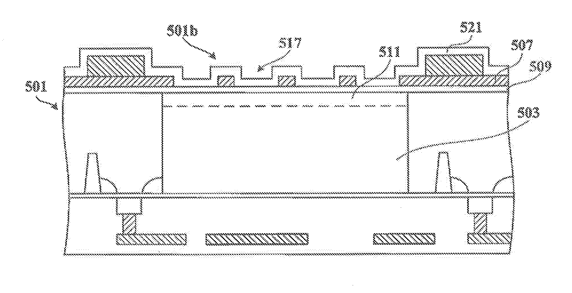
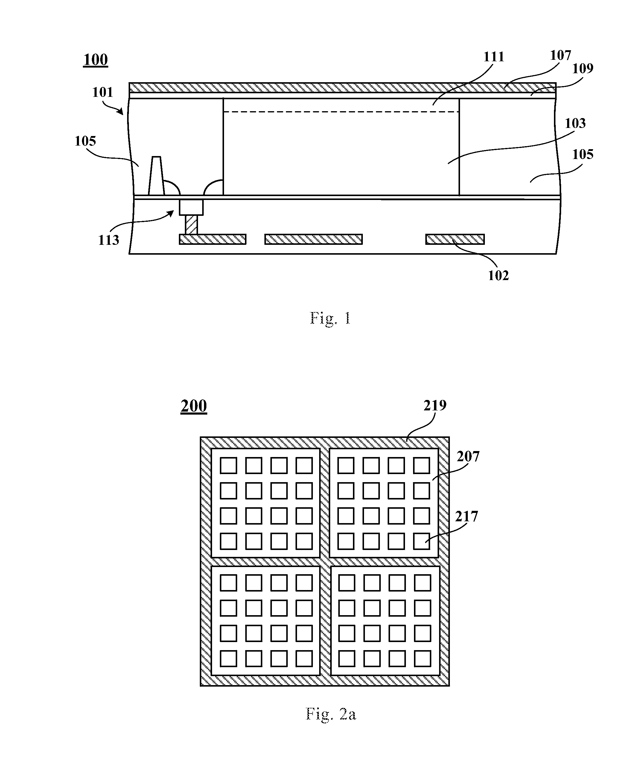
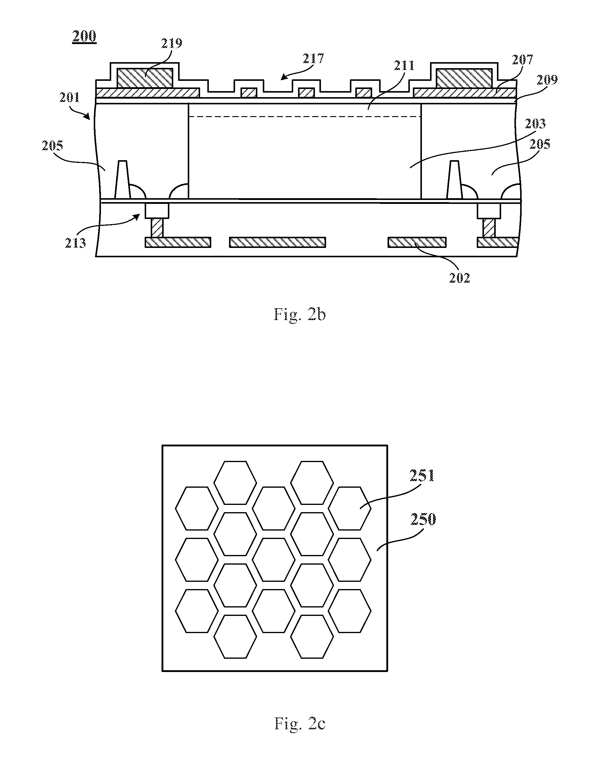
[0032]FIG. 1 illustrates an image sensor 100 according to an embodiment of the invention. The image sensor 100 is a side illumination image sensor. In some embodiments, the image sensor 100 includes one or more pixel elements, each of which can be embodied as a pixel structure including three transistors (3T) or four transistors (4T), i.e., including the photoelectric diode(s) and three or four MOS transistors used to control photo-induced charges to be transferred and to generate an output signal.

[0033]As illustrated in FIG. 1, the image sensor 100 includes: a substrate 101 with a metal interconnection layer 102 formed on a first side thereof;[0034]an N-type doped area 103 located in the substrate 101;[0035]a ...


PUM


Abstract

The invention discloses an image sensor (100) and a method of fabricating the image sensor. The image sensor (100) includes: a substrate (101) with a metal interconnection layer (102) formed on a first side thereof; a first type of doped area (103) located in the substrate (101); a second type of doped area (105) located in the substrate (101) adjacent to the first type of doped area (103) to form a photoelectric diode; an electrode layer (107) located on a second side of the substrate (101), wherein the electrode layer (107) is light-transmissive; and an insulation layer (109) located between the electrode layer (107) and the substrate (101); wherein there is a predetermined potential difference between the electrode layer (107) and the substrate (101) such that a second type of conductive layer (111) is generated on the surface of the second side of the substrate (101).

Description

FIELD OF THE INVENTION[0001]The present disclosure relates to the field of semiconductor technologies and more particularly to an image sensor and a method of fabricating the image sensor.BACKGROUND OF THE INVENTION[0002]Conventional image sensors are typically categorized into a Charge Coupled[0003]Device (CCD) image sensor and a Complementary Metal Oxide Semiconductor (CMOS) image sensor, where the CMOS image sensor has the advantages of a small volume, low power consumption, a low production cost, etc., so it is easy to integrate the CMOS image sensor, for example, in a handset, a notebook computer, a tablet computer and other portable electronic devices as a camera module to provide a digital imaging function.[0004]The CMOS image sensor typically includes photoelectric diodes to collect and convert optical energy into a charge signal. Particularly the surface of a substrate where the photoelectric diodes are formed is doped with ions to form a pinning layer so as to lower dark c...

Claims


Application Information

Patent Timeline
IPC IPC(8): H01L27/146
CPCH01L27/14643H01L27/14683H01L27/14636H01L27/1464H01L27/14603
Inventor ZHAO, LIXINHUO, JIEGUANGLI, JIE
Owner GALAXYCORE SHANGHAI
Why Eureka
Try Eureka