Semiconductor processing method
- Summary
- Abstract
- Description
- Claims
- Application Information
AI Technical Summary
Benefits of technology
Problems solved by technology
Method used
Image


Examples
Embodiment Construction
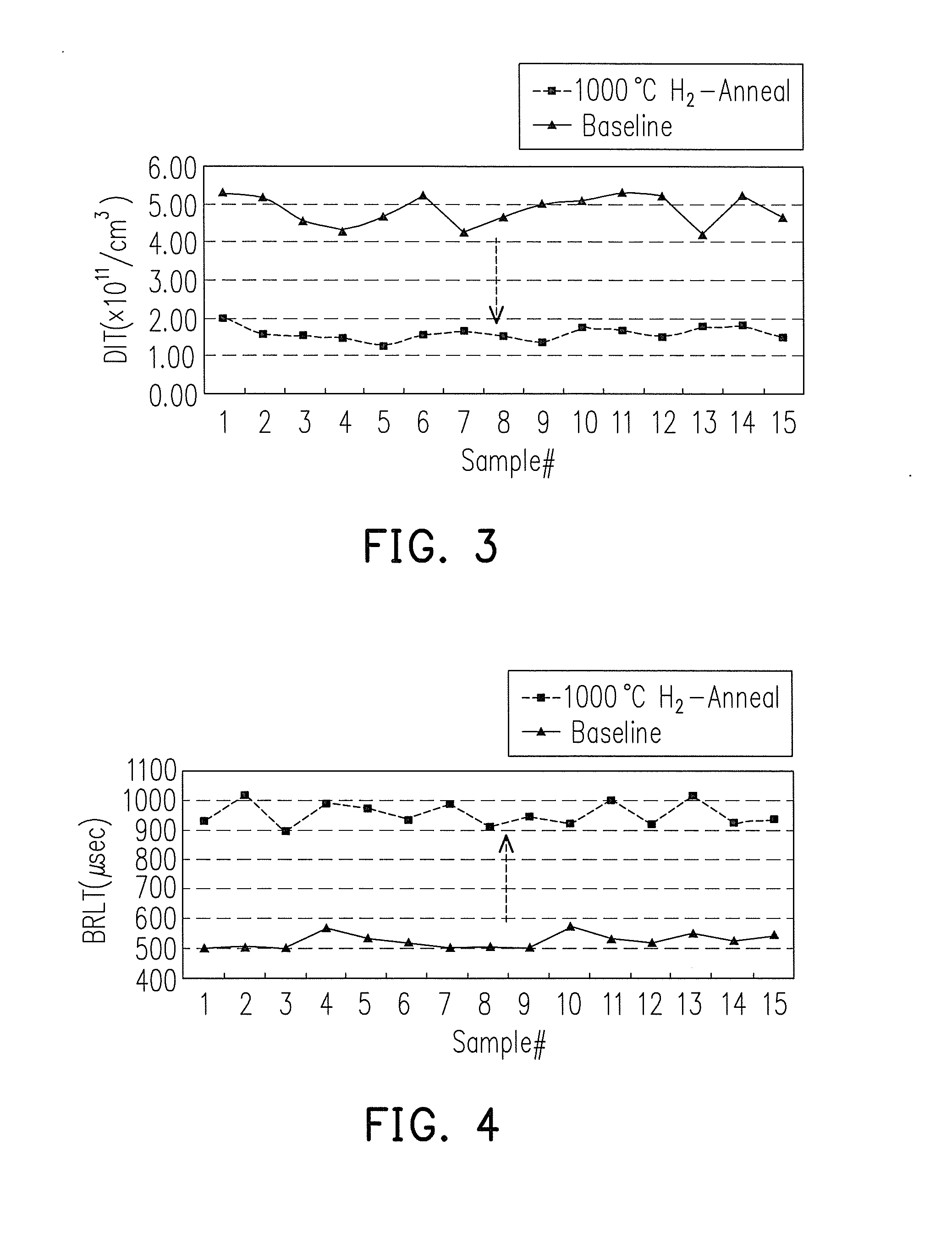
[0014]It is noted that the following embodiment is intended to further explain this invention but not to limit the scope thereof. For example, although in the embodiment a wafer is used and is intended to investigate the metal contamination from the film-forming process, other kind of semiconductor wafer or substrate that has been subjected to a film-forming process causing interface traps may also be treated with the method of this invention, in which the density of interface traps is reduced by the annealing treatment in the method of this invention.
[0015]FIGS. 1A-1C and 2 illustrate a method for detecting metal contamination from a film-forming process causing interface traps according to an embodiment of this invention, wherein FIGS. 1C and 2 illustrate the BRLT measurement step in the method.
[0016]Referring to FIG. 1A, a wafer 10 is provided, which may include single-crystal silicon lightly doped with a p-dopant. A film-forming process causing interface traps is then performed ...
PUM
 Abstract
Description
Claims
Application Information
 - R&D Engineer
- R&D Manager
- IP Professional
- Industry Leading Data Capabilities
- Powerful AI technology
- Patent DNA Extraction
Browse by: Latest US Patents, China's latest patents, Technical Efficacy Thesaurus, Application Domain, Technology Topic.
© 2024 PatSnap. All rights reserved.Legal|Privacy policy|Modern Slavery Act Transparency Statement|Sitemap