Gas barrier film including graphene layer, flexible substrate including the same, and manufacturing method thereof
a technology of gas barrier film and graphene layer, which is applied in the direction of instruments, synthetic resin layered products, transportation and packaging, etc., can solve the problems of difficult use of metal oxide gas barrier films in flexible displays, and the gas barrier film formed of graphene/polymer nano-composite does not provide sufficient gas barrier effect, etc., to achieve excellent gas and water vapor blocking effect and excellent light transmittance
- Summary
- Abstract
- Description
- Claims
- Application Information
AI Technical Summary
Benefits of technology
Problems solved by technology
Method used
Image
Examples
example 1
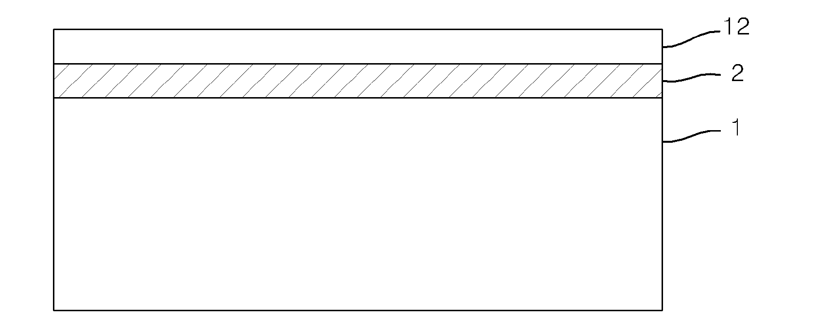
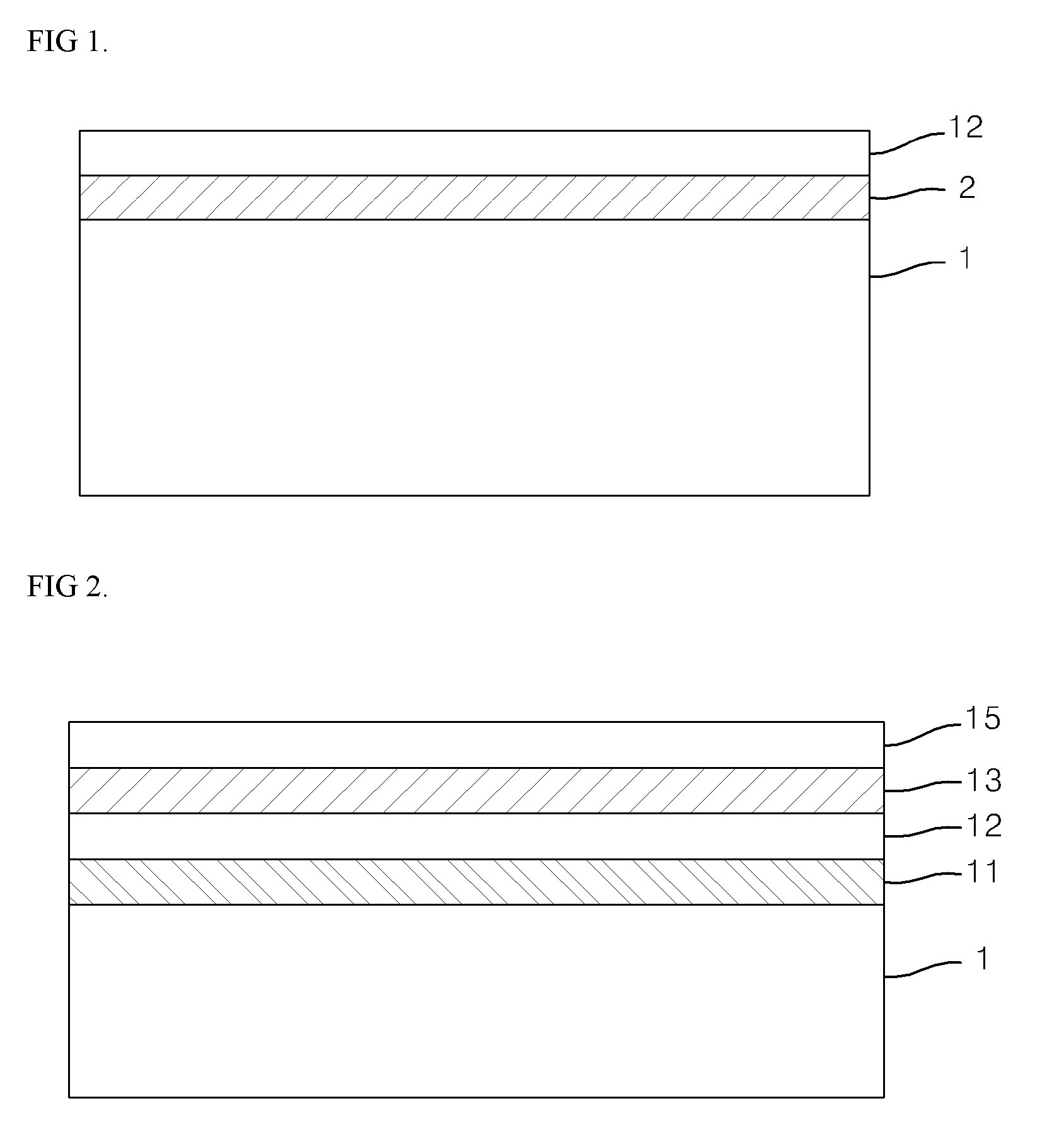
[0094]Graphene was prepared from graphite through oxidation reduction method and a graphene solution containing 0.01 wt % of graphene was prepared. The graphene solution was coated to a thickness of 1 nm onto a 100 μm thick polydimethylsiloxane (PDMS) polymer film using a spin coater to form a first graphene layer. PDMS was coated onto the first graphene layer to a thickness of 1 μm using a spin coater and cured, thereby forming a gas barrier film in which the polymer film, the first graphene layer and the PDMS layer (first organic layer) were sequentially stacked from bottom to top.
example 2
[0095]A second graphene layer (thickness: 1 nm) and a PDMS layer (second organic layer) (thickness: 1 μm) were formed in the same manner on the PDMS layer (first organic layer) of Example 1, thereby forming a gas barrier film in which the polymer film, the first graphene layer, the PDMS layer (first organic layer), the second graphene layer, and the PDMS layer (second organic layer) were sequentially stacked from bottom to top.
example 3
[0096]An aluminum oxide (Al2O3) layer (metal layer) was formed to a thickness of 100 nm on the PDMS layer (first organic layer) of Example 1 by chemical vapor deposition (CVD), and a PDMS layer (second organic layer) was formed thereon to a thickness of 1 μm in the same manner, thereby forming a gas barrier film in which the polymer film, the first graphene layer, the PDMS layer (first organic layer), the aluminum oxide layer (metal layer), and the PDMS layer (second organic layer) were sequentially stacked from bottom to top.
PUM
| Property | Measurement | Unit |
|---|---|---|
| thickness | aaaaa | aaaaa |
| thickness | aaaaa | aaaaa |
| light transmittance | aaaaa | aaaaa |
Abstract
Description
Claims
Application Information
 - R&D
- Intellectual Property
- Life Sciences
- Materials
- Tech Scout
- Unparalleled Data Quality
- Higher Quality Content
- 60% Fewer Hallucinations
Browse by: Latest US Patents, China's latest patents, Technical Efficacy Thesaurus, Application Domain, Technology Topic, Popular Technical Reports.
© 2025 PatSnap. All rights reserved.Legal|Privacy policy|Modern Slavery Act Transparency Statement|Sitemap|About US| Contact US: help@patsnap.com


