Light emitting device on metal foam substrate

a technology of light-emitting devices and metal foam, which is applied in the manufacture of semiconductor/solid-state devices, semiconductor devices, electrical devices, etc., can solve the problems of substrate cost, processing cost limitations, and certain restrictions inherent in thin-film, and achieve the effect of conductive and inexpensiv

Inactive Publication Date: 2014-09-18
THE UNITED STATES OF AMERICA AS REPRESENTED BY THE SECRETARY OF THE NAVY
View PDF3 Cites 3 Cited by
  • Summary
  • Abstract
  • Description
  • Claims
  • Application Information

AI Technical Summary

Benefits of technology

[0015]The subject of this invention allows the design of a light emitting device on a metal foam substrate that is inexpensive, conductive, and can be formed into any reasonable size or shape. The subject can represent a single component in a multiple-component module

Problems solved by technology

Despite this rapid progress, certain restrictions are inherent to the thin-film on a planar substrate design.
These constraints can be generalized into light extraction, defectivity, substrate cost, and processing cost limitations, as well as a lack of mechanical flexibility.
Sapphire is non-conductive, limited in size, and presents a large lattice mismatch with the III-nitride material system.
On the other hand, the silicon carbide substrates are expensive, defective, and limited to four-inches in diameter.
Silicon is available in larger diameters but GaN epitaxy on silicon suffers from thermal stress constraints.
The cost of the wafer is significant but often overstated when compared to the processing and balance of system costs.
Poly-crystal or fine-grain III-nitride material presents an exceedingly large number of dislocations and other defects that effectively destroy operation of the pn junction.
Even for high-quality thin film growth on sapphire, lattice mismatch leads to the formation of dislocations with densities greater than 108 cm−2, which limit the internal quantum efficiency.
Another intrinsic issue with a standard LED structure is the low external extraction efficiency of light owing to the index of contrast difference with air.

Method used


Image

  • Light emitting device on metal foam substrate
  • Light emitting device on metal foam substrate
  • Light emitting device on metal foam substrate

Examples


Embodiment Construction

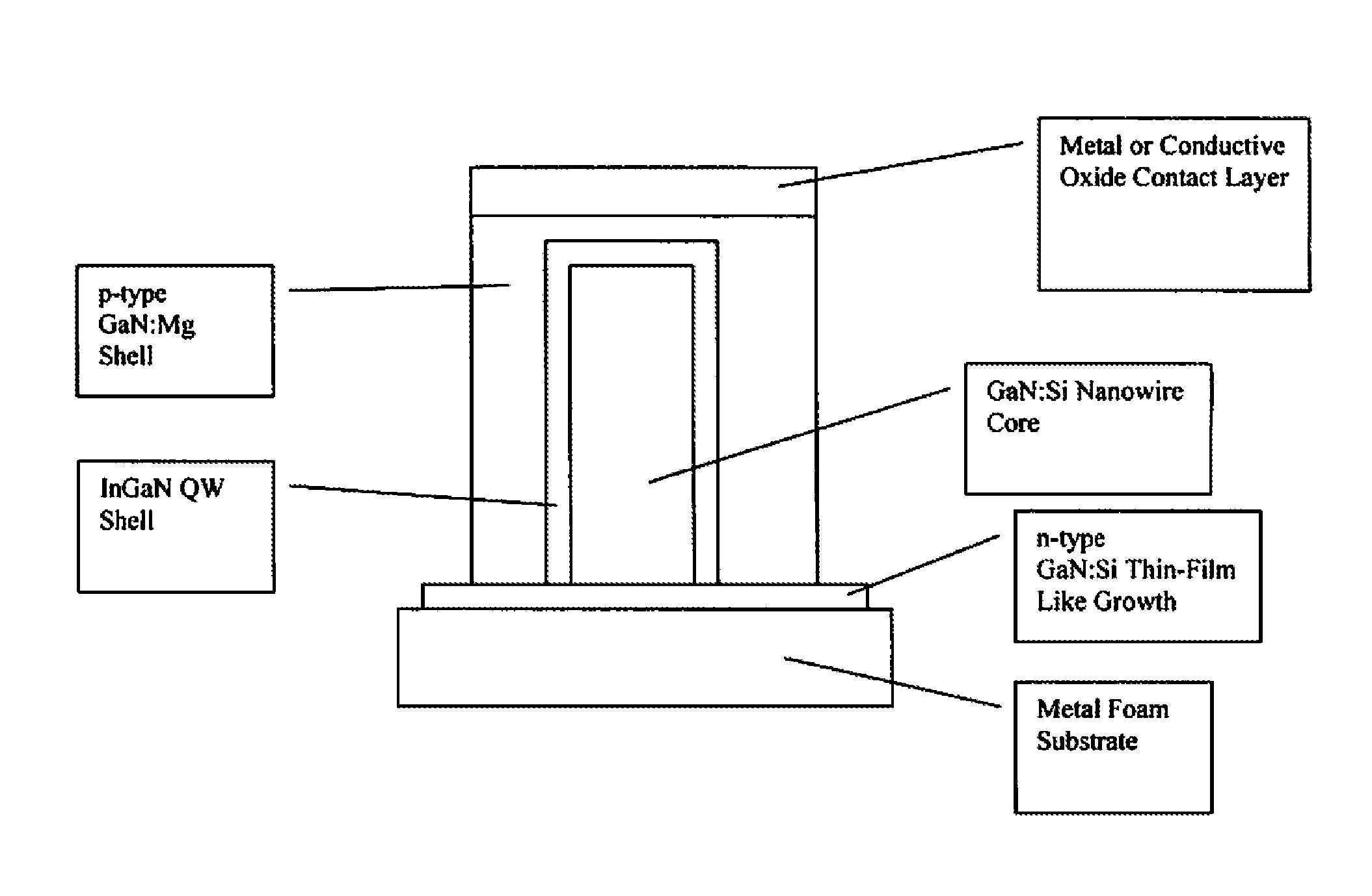
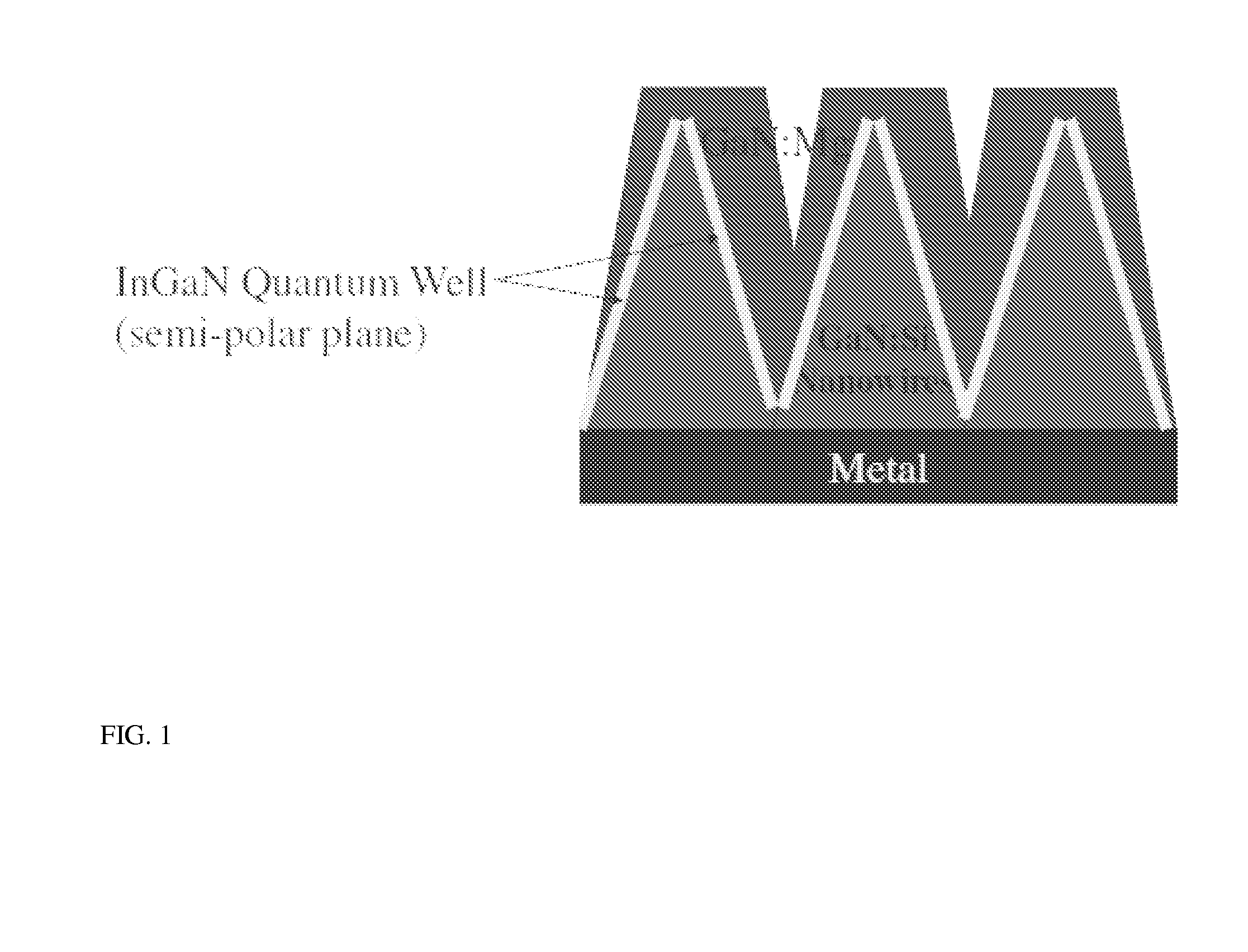
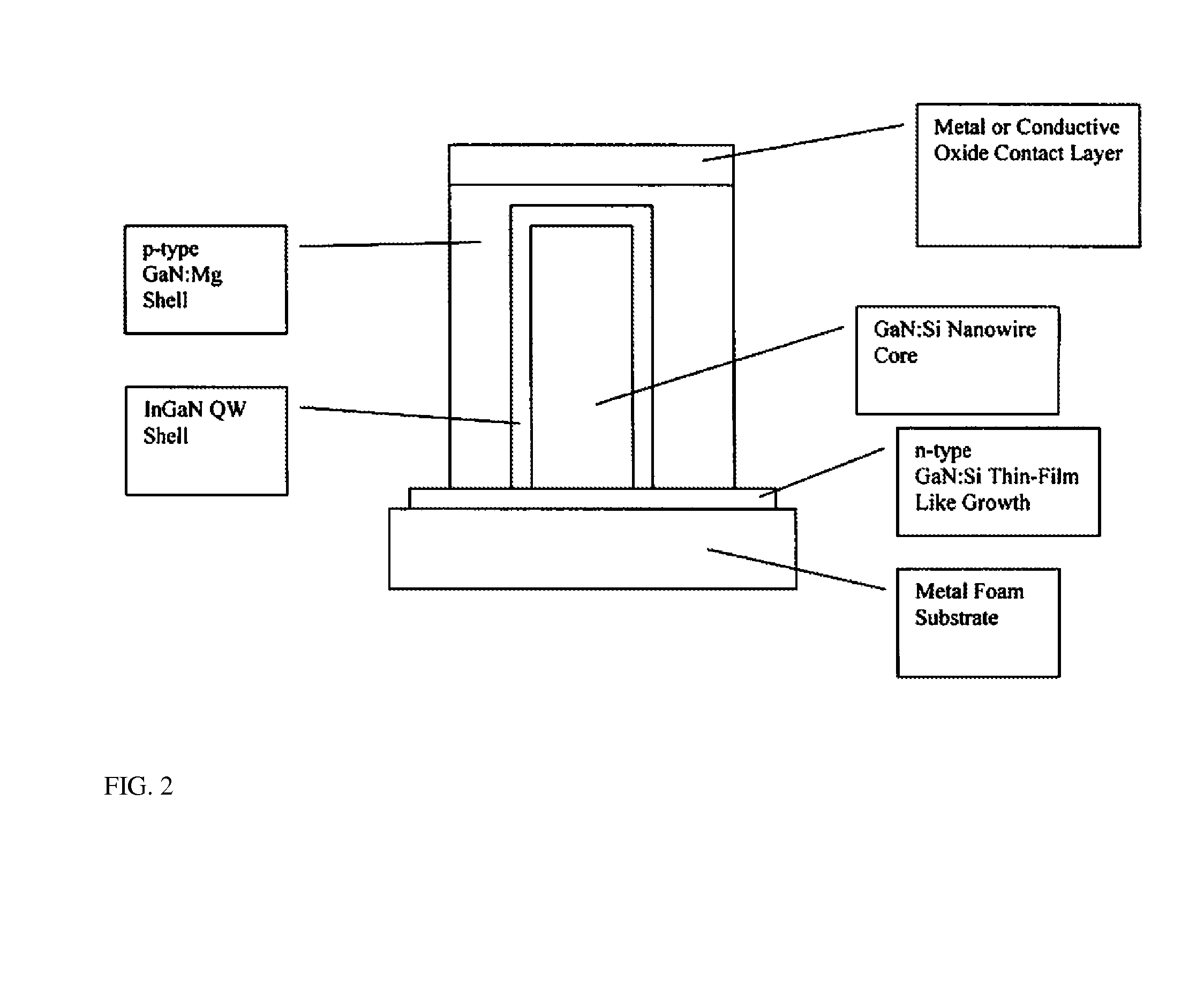
[0024]The present invention provides light emitting nanowire diodes on a metal foam substrate for illumination. The design includes: an electrically conductive metal foam or porous metal substrate; one or more multi-layer semiconductor nanowire light emitting diodes formed in contact with the substrate with a continuous pn junction; a metal coating or conductive oxide layer used to provide an electrical contact to the side of the diode junction opposite the metal substrate; and a package or module to protect and provide electrical or optical stimulation to the device in a continuous or modulated manner. As shown in FIG. 1, the nanowires may have horizontal / vertical growth-regimes that combine to produce a nanowire that is tapered so that the bases of adjacent nanowires touch. As shown, in FIG. 2, there may be an initial thin conformal GaN seed layer formed on the metal substrate by ALE, MOCVD, MBE, PLD or similar technique.

[0025]The substrate can be a metal foam, a porous metal, ali...


PUM

PropertyMeasurementUnit
pore diametersaaaaaaaaaa
diameteraaaaaaaaaa
lengthaaaaaaaaaa

Abstract

A light emitting device having an electrically conductive metal foam or porous metal substrate, one or more light emitting nanowires in contact with the substrate, and a metal or conductive oxide contact layer in contact with each nanowire junction opposite of the substrate. More specifically, a light emitting device having an electrically conductive metal foam substrate, one or more light emitting nanowires in contact with the substrate, a quantum well on the nanowire(s), a p-type shell on the quantum well, a metal or conductive oxide contact layer in contact with the shell, and an energy down-converting material. Also disclosed is the related method of making a light emitting device.

Description

PRIORITY CLAIM[0001]The present application is a non-provisional application claiming the benefit of U.S. Provisional Application No. 61 / 781,652, filed on Mar. 14, 2013 by Michael A. Mastro et al., entitled “Light Emitting Device on Metal Foam Substrate,” the entire contents of which is incorporated herein by reference.BACKGROUND OF THE INVENTION[0002]1. Field of the Invention[0003]The present invention relates generally to light emitting diodes and, more specifically, to light emitting devices on a metal foam substrate.[0004]2. Description of the Prior Art[0005]The GaN-based light emitting diode (LED) market has grown into a multi-billion dollar market in just two decades. Despite this rapid progress, certain restrictions are inherent to the thin-film on a planar substrate design. These constraints can be generalized into light extraction, defectivity, substrate cost, and processing cost limitations, as well as a lack of mechanical flexibility.[0006]Sapphire is the predominant subs...

Claims


Application Information

Patent Timeline
Patent Type & Authority Applications(United States)
IPC IPC(8): H01L33/06
CPCH01L33/06H01L21/02425H01L21/02428H01L21/02458H01L21/02521H01L21/0254H01L21/02603H01L21/02653H01L33/005H01L33/02H01L33/24
Inventor MASTRO, MICHAEL A.KUB, FRANCIS J.
Owner THE UNITED STATES OF AMERICA AS REPRESENTED BY THE SECRETARY OF THE NAVY
Why Eureka
Try Eureka