Composite Substrate
a technology of composite substrates and substrates, applied in piezoelectric/electrostrictive/magnetostrictive devices, piezoelectric/electrostriction/magnetostriction machines, electrical apparatus, etc., can solve the problems of small electromechanical coupling coefficient and poor temperature stability, and achieve the effect of improving adhesion strength, reducing thermal stress, and improving adhesion strength
- Summary
- Abstract
- Description
- Claims
- Application Information
AI Technical Summary
Benefits of technology
Problems solved by technology
Method used
Image
Examples
example 1
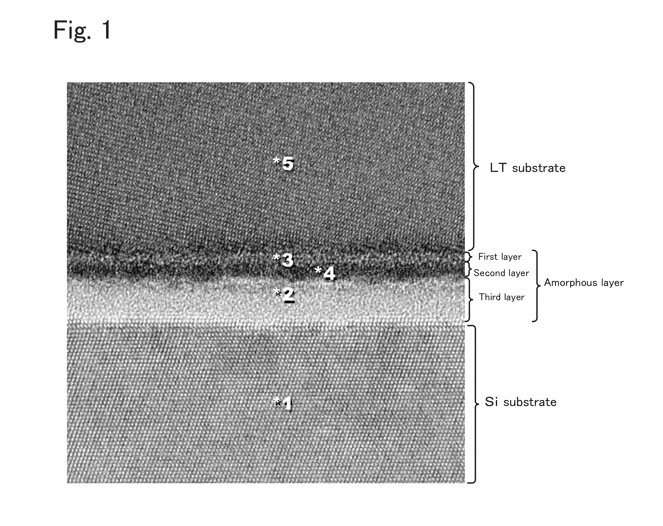
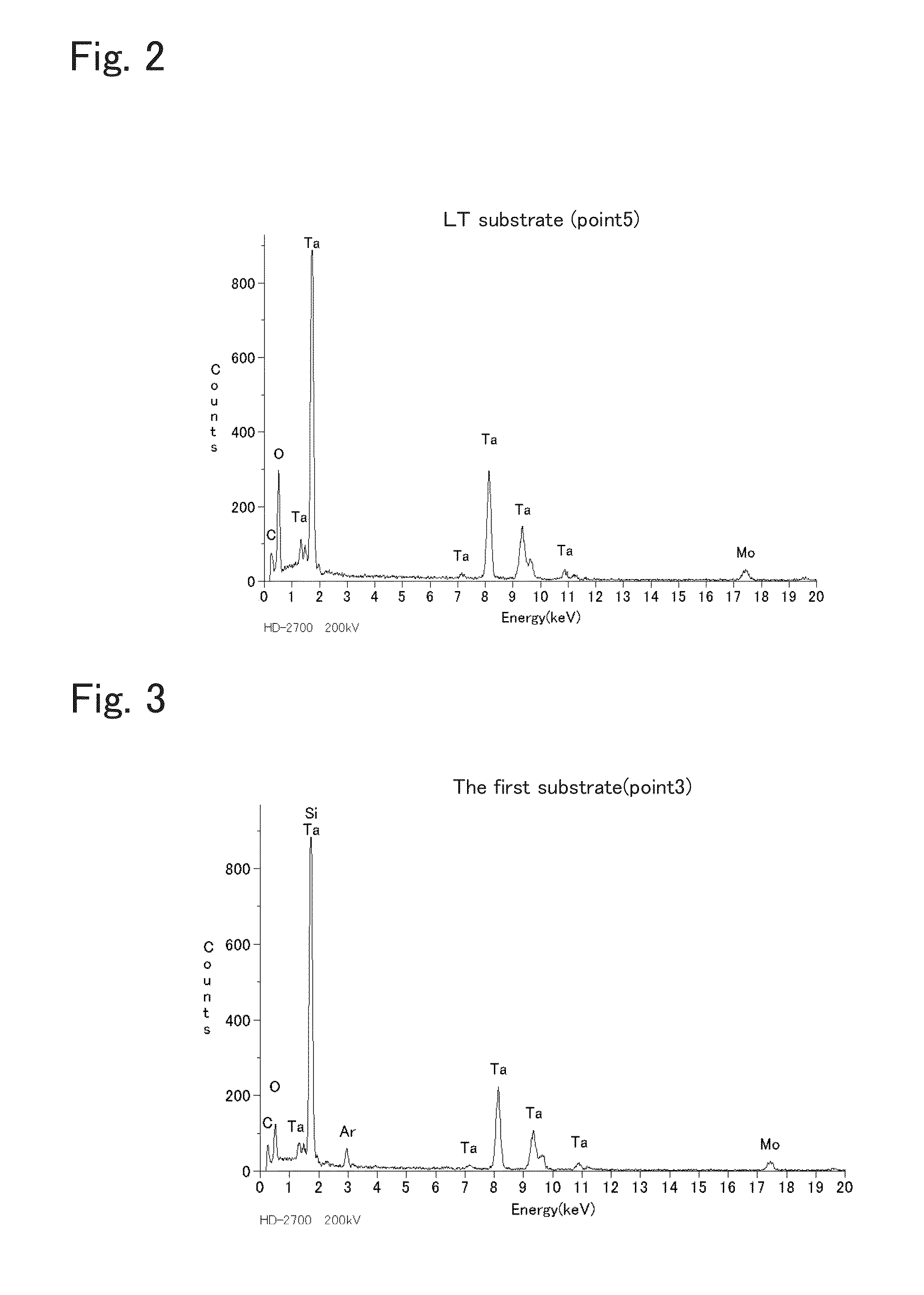
[0043]An LT substrate having a mirror finish on each side thereof and having a thickness of 230 μm and a silicon substrate having a mirror finish on each side thereof and having a thickness of 250 μm were prepared. The LT substrate used was a 42°-rotated Y-cut X-propagation LT substrate (42° Y-X LT), which is rotated by 42° from the Y axis toward the Z axis about the X axis, which is the direction in which a surface acoustic wave propagates. After the joining surface of each substrate was cleaned to remove soil therefrom, it was introduced into a vacuum chamber. The joining surface of each substrate was irradiated with a high-speed neutral argon atom beam (at an acceleration voltage of 1 kV and an argon flow rate of 60 sccm) in a vacuum on the order of 10−6 Pa for 70 seconds. After irradiation, each substrate was left standing for 10 minutes to cool the substrate to 26° C. to 28° C. The LT substrate and the silicon substrate were then joined together by bringing into contact the sur...
example 2
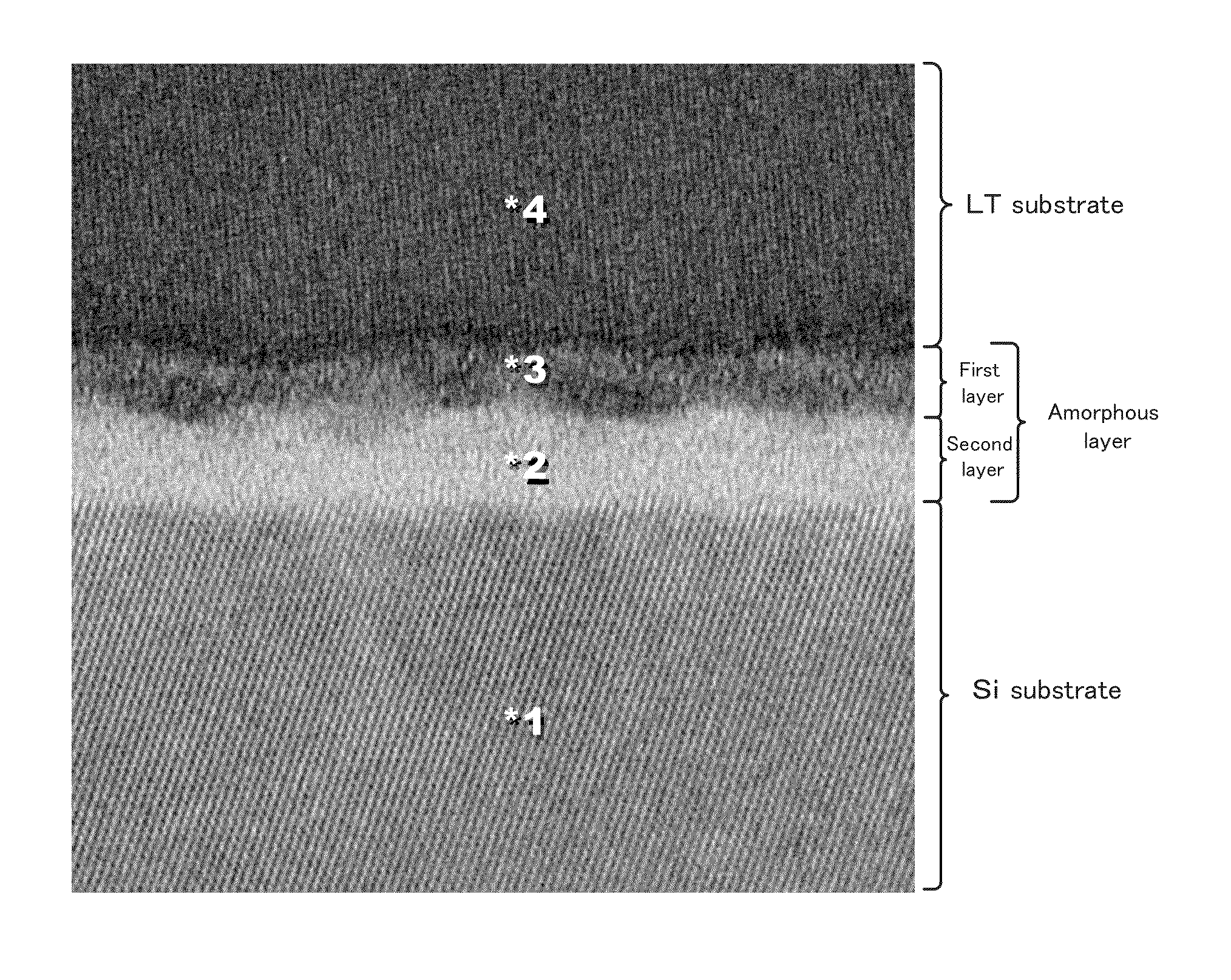
[0045]A composite substrate was manufactured as in Example 1 except that each substrate was irradiated with a high-speed neutral argon atom beam for 20 seconds, and a portion thereof was cut to examine a cross-section under a TEM. As a result, the amorphous layer had a thickness of about 4 nm. The amorphous layer included, in order from the LT substrate toward the silicon substrate, a first layer, a second layer, and a third layer. The third layer was thicker than the first and second layers. The LT substrate, the first to third layers of the amorphous layer, and the silicon substrate were examined by composition analysis and elemental analysis using EDX. According to the composition analysis, argon was detected in all of the first to third layers. According to the elemental analysis, the first layer contained 1.5 atomic percent of argon atoms, the second layer contained 3.9 atomic percent of argon atoms, and the third layer contained 0.7 atomic percent of argon atoms. No iron atoms...
example 3
[0046]A composite substrate was manufactured as in Example 1 except that each substrate was irradiated with a high-speed neutral argon atom beam for 265 seconds, and a portion thereof was cut to examine a cross-section under a TEM. As a result, the amorphous layer had a thickness of about 12 nm. The amorphous layer included, in order from the LT substrate toward the silicon substrate, a first layer, a second layer, and a third layer. The third layer was thicker than the first and second layers. The LT substrate, the first to third layers of the amorphous layer, and the silicon substrate were examined by composition analysis and elemental analysis using EDX. According to the composition analysis, argon was detected in all of the first to third layers. According to the elemental analysis, the first layer contained 10.8 atomic percent of argon atoms, the second layer contained 16.3 atomic percent of argon atoms, and the third layer contained 8.4 atomic percent of argon atoms. No iron a...
PUM
| Property | Measurement | Unit |
|---|---|---|
| thickness | aaaaa | aaaaa |
| temperature | aaaaa | aaaaa |
| temperature | aaaaa | aaaaa |
Abstract
Description
Claims
Application Information
 - R&D
- Intellectual Property
- Life Sciences
- Materials
- Tech Scout
- Unparalleled Data Quality
- Higher Quality Content
- 60% Fewer Hallucinations
Browse by: Latest US Patents, China's latest patents, Technical Efficacy Thesaurus, Application Domain, Technology Topic, Popular Technical Reports.
© 2025 PatSnap. All rights reserved.Legal|Privacy policy|Modern Slavery Act Transparency Statement|Sitemap|About US| Contact US: help@patsnap.com


