Method of fabricating a perfluorosulfonated ionomer membrane with a molecular alignment
a technology of perfluorosulfonated ionomer and ionomer membrane, which is applied in the direction of sustainable manufacturing/processing, final product manufacturing, electrochemical generators, etc., can solve the problems of low humidity, high proton transport resistance in fine bumps, and the prior art disclosed in the prior art, etc., to achieve rapid deformation of the membrane surface, improve performance, and reduce proton transport resistance
- Summary
- Abstract
- Description
- Claims
- Application Information
AI Technical Summary
Benefits of technology
Problems solved by technology
Method used
Image
Examples
example 1
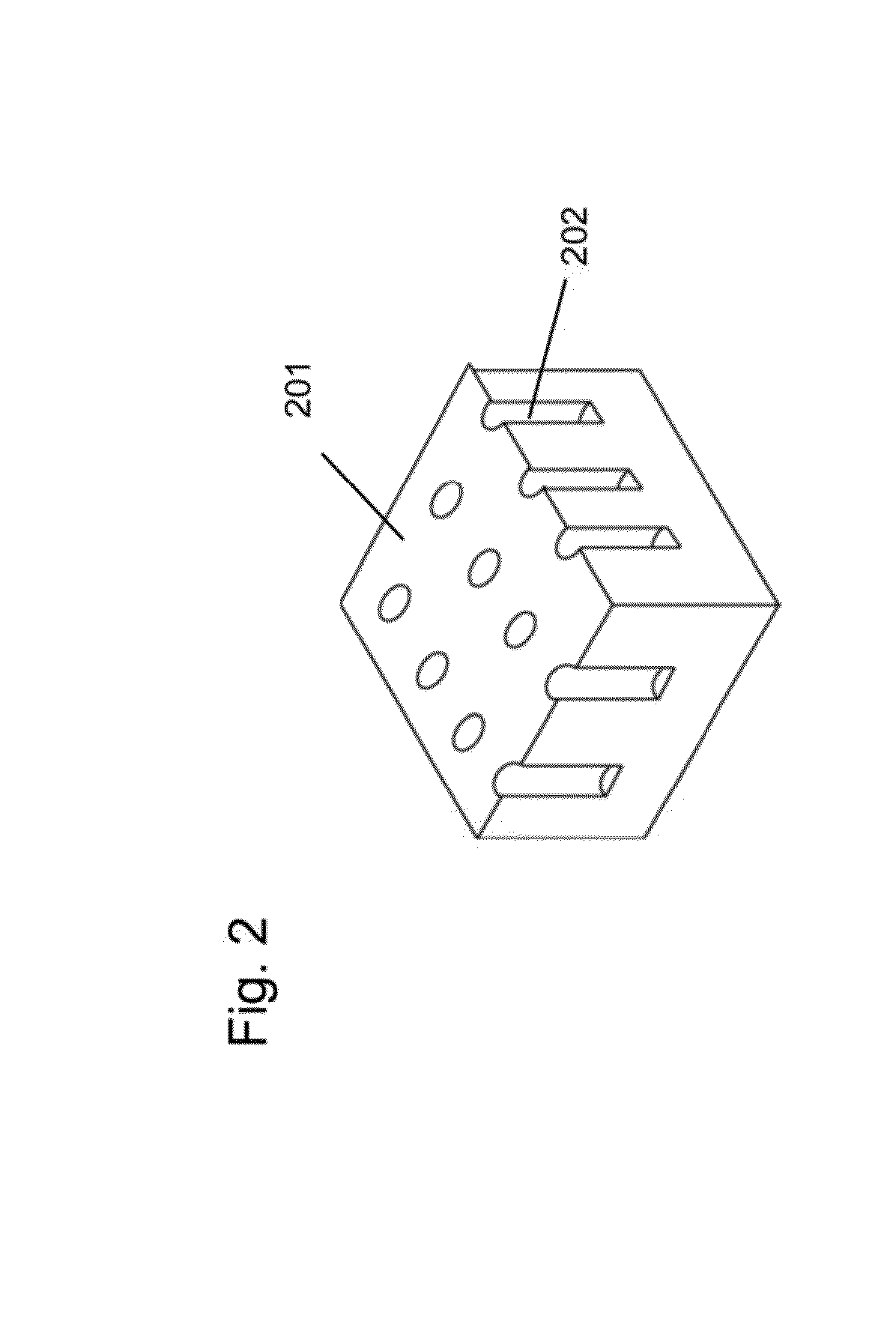
[0076]Photolithography based on a BOSCH etching process was performed to form a periodic tapered hole structure on a 4″ single crystal Si wafer. An area having the hole structure was 60 mm×60 mm. FIG. 9 shows a cross-sectional view of the hole structure. The tapered holes have an upper-width of 2.5 micrometers, a bottom-width of 1.9 micrometers, a depth of 7.0 micrometers, and an inter-hole distance of 6.0 micrometers.
[0077]A silicon mold for thermal imprint lithography was fabricated by cutting out the hole structure region from the wafer. The mold was degreased in ethanol, followed by acetone. Then, it was further cleaned by a UV-ozone stripper at 110° C. for 10 min. A self-assembled monolayer (SAM) of fluorinated polymer (NANOS B, T&K Corp.) was deposited on the mold by vacuum evaporation.
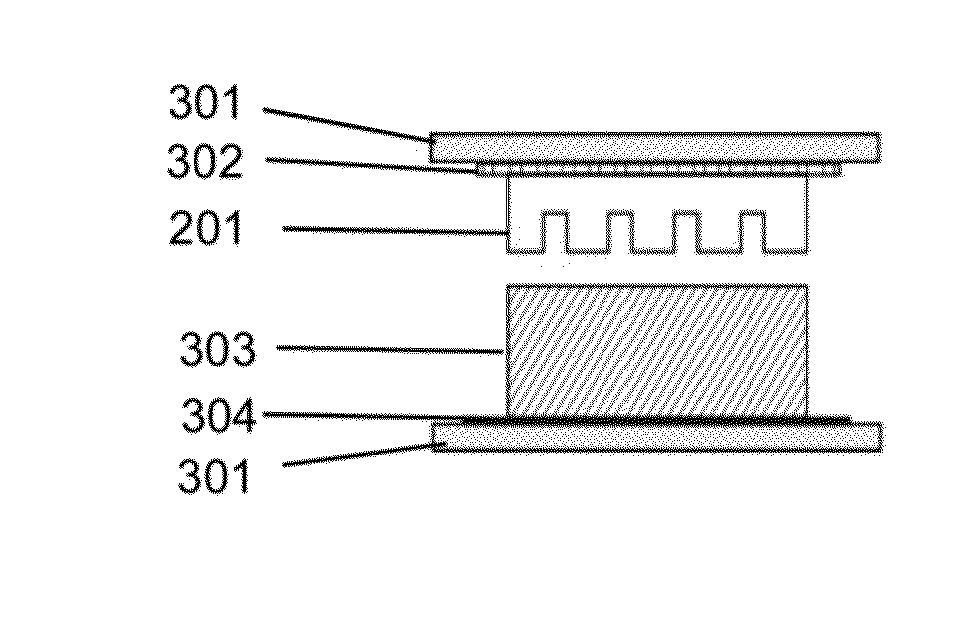
[0078]Thermal imprinting of a PFSI membrane was performed in the experimental setup shown in FIG. 3. A 150 mm×150 mm Nafion membrane with 50 micrometers thickness (NRE212, DuPont Corp.) was heat...
example 2
[0081]The same fabrication procedures described in Example 1 produced a silicon mold with its surface having an array of plurality of holes. The holes had the same upper and bottom width, and inter-hole distance as those described in Example 1 but a different depth of 10.1 micrometers. The thermal imprint process utilized in Example 1 was also applied to a Nafion membrane using the mold. A surface of the resulting membrane had an array of a plurality of pillars, each of which has the same upper and bottom width, and inter-pillar distance as those described in Example 1 but a different height of 10.1 micrometers. The term “same” used above means the agreement within an experimental error of ±0.5 micrometers.
example 3
[0082]The same fabrication procedures described in Example 1 produced a silicon mold with its surface having an array of plurality of holes. The holes had the same upper and bottom width, and inter-hole distance as those described in Example 1 but a different depth of 3.1 micrometers. The thermal imprint process utilized in Example 1 was applied to a Nafion membrane using the mold. A surface of the resulting membrane had an array of a plurality of pillars, each of which has the same upper and bottom width as those described in Example 1 but a different height of 3.1 micrometers.
PUM
| Property | Measurement | Unit |
|---|---|---|
| Temperature | aaaaa | aaaaa |
| Temperature | aaaaa | aaaaa |
| Temperature | aaaaa | aaaaa |
Abstract
Description
Claims
Application Information
 - R&D
- Intellectual Property
- Life Sciences
- Materials
- Tech Scout
- Unparalleled Data Quality
- Higher Quality Content
- 60% Fewer Hallucinations
Browse by: Latest US Patents, China's latest patents, Technical Efficacy Thesaurus, Application Domain, Technology Topic, Popular Technical Reports.
© 2025 PatSnap. All rights reserved.Legal|Privacy policy|Modern Slavery Act Transparency Statement|Sitemap|About US| Contact US: help@patsnap.com


