Lead frame

a lead frame and frame technology, applied in the association of printed circuit non-printed electric components, basic electric elements, solid-state devices, etc., can solve the problems of etching process difficulty, neighboring parts cannot tolerate external force, and may produce cutting burrs, etc., to prolong the life of the rotary blade, suppress the production of cutting burrs, and enhance the strength

Active Publication Date: 2014-07-17
MITSUI HIGH TEC INC
View PDF4 Cites 5 Cited by
  • Summary
  • Abstract
  • Description
  • Claims
  • Application Information

AI Technical Summary

Benefits of technology

[0010]The present invention has been made in consideration with the above circumstance, and an object of the present invention is to provide a lead frame having a connecting bar, the shape of which can be formed with simple etching process, so as to suppress the production of cutting burr in dicing and to prevent a periphery of a crossing point of connecting bars from being deformed.
[0017]According to the lead frame as mentioned above, the thickness of metal of the dicing part to be cut with the rotary blade is thinned. Since a load to the rotary blade applied when performing dicing is reduced, production of cutting burr is suppressed and a life of the rotary blade is prolonged. Further, since the strength retention part is formed in the half-etching part and extended from the crossing part of the connecting bar to the end lead located closest to the crossing part among the leads of the unit lead frame adjacent to the crossing part, it is possible to enhance the strength on a part on which a stress is most likely concentrated. Thus, it is unnecessary more than necessary to increase the thickness of the metal in the dicing part, and the lead frame is prevented from being deformed. In addition, since the strength of the lead frame is increased, it is harmonized with growing in size of the semiconductor apparatus and the thinning of the lead frame. In addition, since the strength retention part includes the first strength retention part and the second strength retention part, the connecting bar is tolerant to a stress applied from multi-directions, and moreover, etching process becomes simple for a part between the first strength retention part and a widthwise end of the half-etching part of the lead.

Problems solved by technology

Accordingly, in a structure in which the whole of the connecting bar is thinned as described in JP-A-2005-166695, a problem is raised that the connecting bar, which serves as a connection of the unit lead frames, and its neighboring parts cannot be tolerant to an external force, thereby being deformed.
In this method, however, although the strength of the dam bar is secured, since the thicker part is formed consecutively to the dam bar, a problem is raised that the cutting burr may be produced because the load to the rotary blade cannot be sufficiently lowered when performing dicing.
In addition, an etching process becomes difficult because an etching solution is hardly infiltrated into a portion to be etched which is provided between the lead and the portion thicker than the thinned portion.

Method used


Image

  • Lead frame
  • Lead frame
  • Lead frame

Examples


Embodiment Construction

[0026]A lead frame according to exemplary embodiments of the present invention will be described in detail with reference to the accompanying drawings.

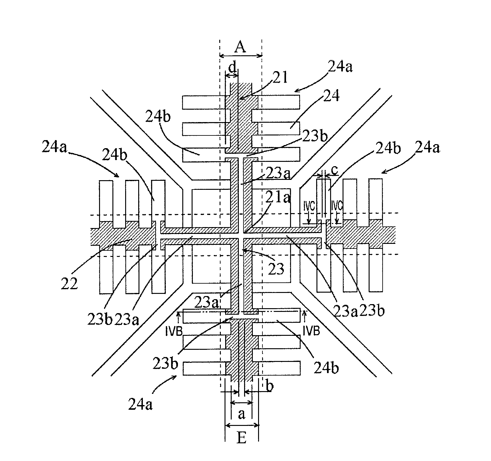
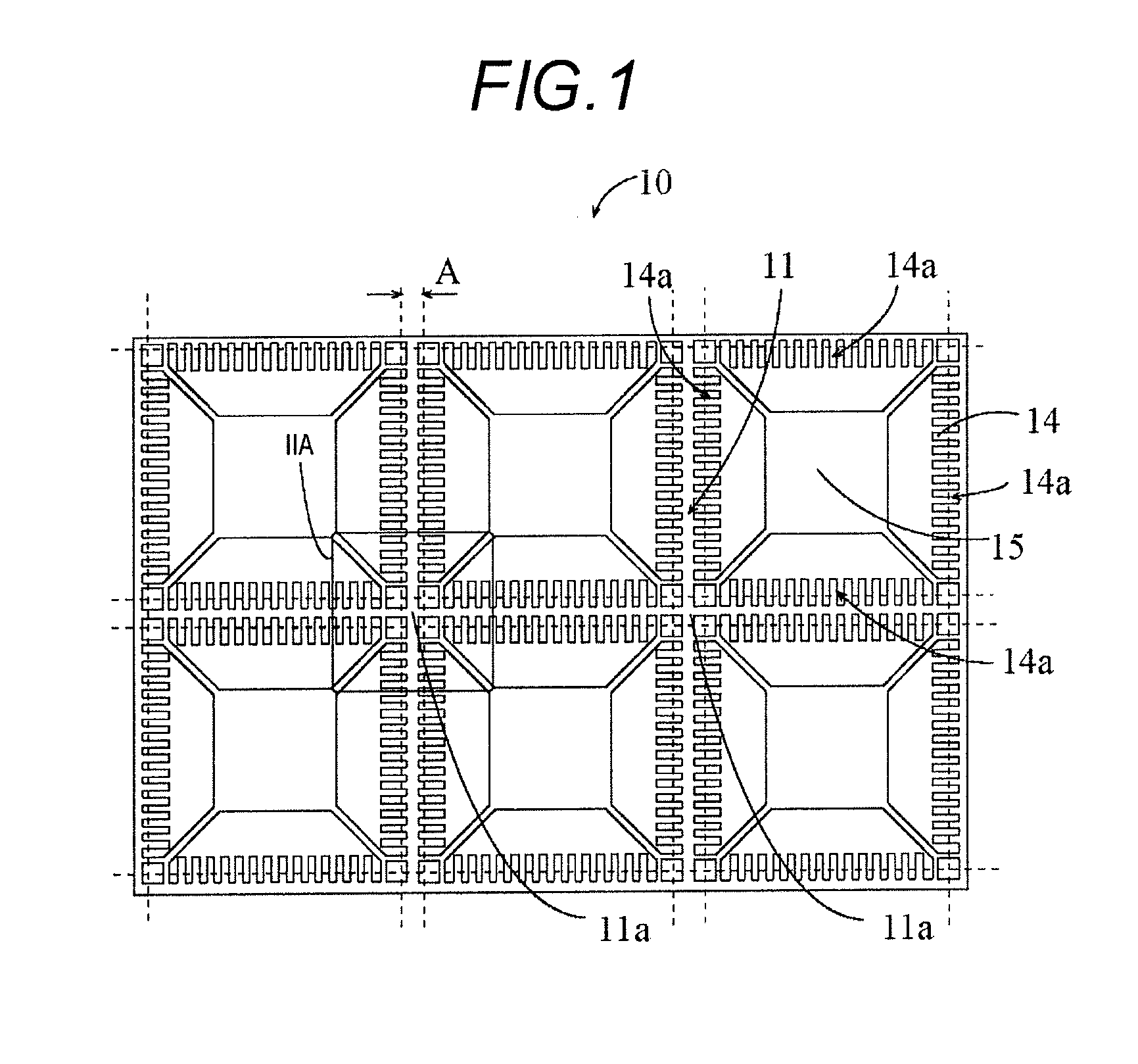
[0027]FIG. 1 is a schematic plan view of a lead frame 10 according to a first embodiment of the present invention. The lead frame 10 includes a plurality of unit lead frames arranged in a matrix. Each unit lead frame includes a mounting part 15 on which a semiconductor device 16 is mounted. The unit lead frame includes a plurality of leads 14, being divided into four lead groups 14a aligned along each side of the unit lead frame. The leads 14 of adjacent unit lead frames are connected via a connecting bar 11. The connecting bar 11 includes a longitudinal connecting bar and a transverse connecting bar. The longitudinal connecting bar and the transverse connecting bar cross each other at a crossing part 11a. A dashed line indicates a dicing line to be cut with a rotary blade after one surface of the lead frame 10 is sealed with resin 18...


PUM


Abstract

A lead frame includes a plurality of unit lead frames arranged in a matrix. Leads of adjacent ones of the unit lead frames are connected via a connecting bar, in which a longitudinal connecting bar and a transverse connecting bar are crossed at a crossing part. The lead frame further includes a dicing part including the connecting bar and a part of the leads, to be cut along a dicing line, a half-etching part formed along the dicing part, and being smaller in width than the dicing part, and a strength retention part formed in the half-etching part and extended from the crossing part of the connecting bar at least to an end lead located closest to the crossing part among the leads of the unit lead frame adjacent to the crossing part.

Description

CROSS-REFERENCE TO RELATED APPLICATIONS[0001]This application is based upon and claims the benefit of priority of Japanese Patent Application No. 2013-003110 filed on Jan. 11, 2013, the contents of which are incorporated herein by reference in its entirety.BACKGROUND OF THE INVENTION[0002]1. Field of the Invention[0003]The present invention relates to a lead frame used for a semiconductor apparatus, especially for a QFN (Quad Flat Non-Leaded) semiconductor apparatus which is manufactured using a MAP (Molded Array Process) mold-forming technique in which a plurality of semiconductor apparatuses are collectively sealed with resin.[0004]2. Description of the Related Art[0005]A QFN semiconductor apparatus is manufactured by using the MAP mold-forming technique which seals a plurality of semiconductor apparatuses with resin collectively. First, a lead frame in which a plurality of lead parts of adjacent unit lead frames are interconnected via a connecting bar is prepared as a MAP lead fr...

Claims


Application Information

Patent Timeline
Patent Type & Authority Applications(United States)
IPC IPC(8): H01L23/495
CPCH01L23/49537H01L23/49586H01L21/561H01L23/3107H01L23/49541H01L23/49562H01L24/32H01L24/48H01L24/73H01L24/97H01L2224/32245H01L2224/48091H01L2224/48247H01L2224/73265H01L2224/97H01L2924/00014H01L2924/181H01L2924/18165H05K1/18H05K1/181H05K3/0052
Inventor ISHIBASHI, TAKAHIRO
Owner MITSUI HIGH TEC INC
Why Eureka
Try Eureka