Unipolar programmable metallization cell

a metallization cell, unipolar technology, applied in the direction of digital storage, instruments, electrical apparatus, etc., can solve the problems of complex peripheral circuitry, reduced array density, and inability to adapt to many 3d memory structures

Active Publication Date: 2014-05-15
MACRONIX INT CO LTD
View PDF3 Cites 51 Cited by
  • Summary
  • Abstract
  • Description
  • Claims
  • Application Information

AI Technical Summary

Benefits of technology

The patent describes a memory device that operates using unipolar principles. It includes a programmable metallization cell (PMC) with a thermal reset structure. The device consists of several layers including a first electrode, a second electrode, a dielectric layer, a conductive ion-barrier layer, and an ion-supplying layer. The conductive ion-barrier layer blocks ion diffusion during reset operations while allowing sufficient ion diffusion during set operations. The dielectric layer supports the formation of conducting bridges through the use of ions from the ion-supplying layer. The device can include supporting circuitry to apply different bias conditions to induce the formation of conducting bridges and the thermal disintegration of bridges. The memory device can be formed in an array and can be accessed using biased voltages to set the memory structure. The array can include cross-point or three-dimensional arrangements of memory cells and diode access devices. The technical effects of this invention include a more efficient and reliable memory device that can be easily accessed and programmed using unipolar principles.

Problems solved by technology

Where transistors are required access devices, the density of the array is reduced, and the peripheral circuitry is complex.
Also, the isolation device / memory element approach is not suitable for many 3D memory structures, including so called Bit Cost Scalable BiCS structures and other 3D memory structures that include a large number of memory layers.

Method used


Image

  • Unipolar programmable metallization cell
  • Unipolar programmable metallization cell
  • Unipolar programmable metallization cell

Examples


Embodiment Construction

[0020]A detailed description of embodiments of the present invention is provided with reference to the FIGS. 1-7.

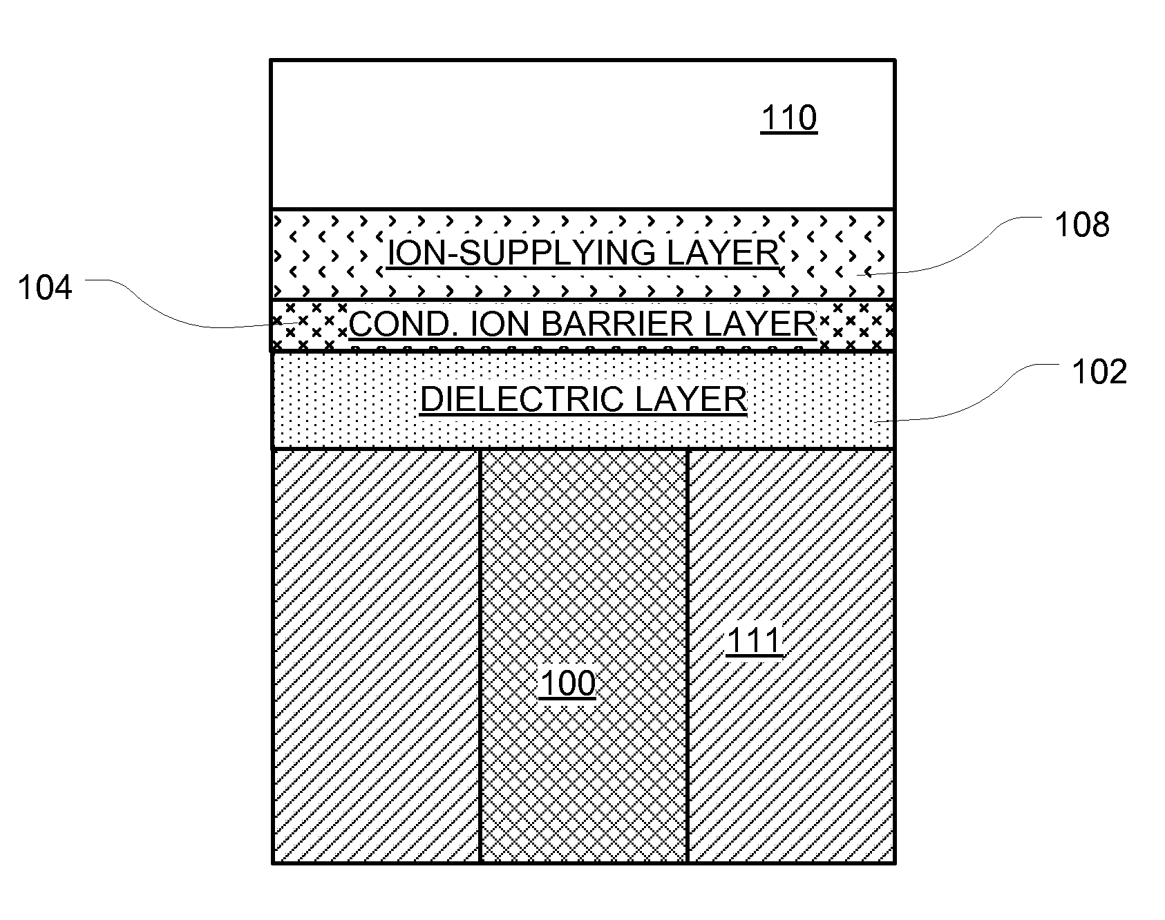
[0021]FIG. 1 illustrates a cross-sectional view of a PMC cell including a thermal reset structure. The PMC cell includes a first electrode 100, which in this example comprises a plug within a via through an interlayer dielectric 111. The cell includes a dielectric layer 102 overlying and contacting the first electrode 100. The dielectric layer 102 can be comprised of any dielectric material that is suitable for allowing the diffusion of conductive ions through the layer, and formation of a conductive bridge through the PMC cell. Such dielectric layers can be silicon dioxide, silicon nitride, silicon oxynitride, metal oxides, high-K dielectric materials and other materials that can support electrolytic formation and destruction of conducting bridges therethrough.

[0022]A conductive ion-barrier layer 104 overlies the dielectric layer 102. The conductive ion-barrier layer 104...


PUM


Abstract

A programmable metallization device comprises a first electrode and a second electrode, and a dielectric layer, a conductive ion-barrier layer, and an ion-supplying layer in series between the first and second electrodes. In operation, a conductive bridge is formed or destructed in the dielectric layer to represent a data value using bias voltages having the same polarity, enabling the use of diode access devices. To form a conductive bridge, a bias is applied that is high enough to cause ions to penetrate the conductive ion-barrier layer into the dielectric layer, which then form filaments or bridges. To destruct the conductive bridge, a bias of the same polarity is applied that causes current to flow through the structure, while ion flow is blocked by the conductive ion-barrier layer. As a result of Joule heating, any bridge in the dielectric layer disintegrates.

Description

BACKGROUND OF THE INVENTION[0001]1. Field of the Invention[0002]The present invention relates to programmable metallization cell (PMC) technology.[0003]2. Description of Related Art[0004]Programmable Metallization Cell (PMC) technology is being investigated for use in nonvolatile memory, reconfigurable logic, and other switching applications due to its low current, good scalability, and high programming speed. The resistance switching of PMC devices is manifested by growing and removing conducting bridges through an electrochemical or electrolytic process. Therefore, PMC devices have also been referred to as conducting bridge (CB) devices or electrochemical (EC) devices.[0005]PMC devices have an ON state in which the conductive bridge completes a current path between electrodes, and an OFF state in which the conductive bridge is reduced such that it does not complete a current path between the electrodes. Such PCM cells have a bipolar operating characteristic. As a result, when arra...

Claims


Application Information

Patent Timeline
IPC IPC(8): H01L45/00G11C11/00
CPCG11C11/00H01L45/00H10B63/20H10N70/245H10N70/8416H10N70/883H10N70/826
Inventor LEE, FENG-MINGLIN, YU-YULEE, MING-HSIU
Owner MACRONIX INT CO LTD
Why Eureka
Try Eureka