Devices and circuits with programmable metallization cells and methods of operation and manufacture thereof

A technology of metallization and storage unit, which is applied in the fields of storage devices and integrated circuits and their operation and manufacture, and can solve the problems of increasing the thickness and/or area of ​​storage structures by separating devices

Active Publication Date: 2016-08-03
MACRONIX INT CO LTD
View PDF5 Cites 0 Cited by
  • Summary
  • Abstract
  • Description
  • Claims
  • Application Information

AI Technical Summary

Problems solved by technology

Separators add additional process and storage structure thickness and / or area

Method used


Image

  • Devices and circuits with programmable metallization cells and methods of operation and manufacture thereof
  • Devices and circuits with programmable metallization cells and methods of operation and manufacture thereof
  • Devices and circuits with programmable metallization cells and methods of operation and manufacture thereof

Examples


Embodiment Construction

[0065] The following examples are given in particular, and in conjunction with the attached Figure 1 to Figure 11 , as detailed below.

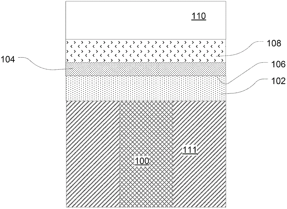
[0066] figure 1 A cross-sectional view of a programmable metallization unit with two dielectric layers according to an embodiment of the invention is shown. The programmable metallization unit includes a first electrode 100 , and in an embodiment, the first electrode 100 includes a plug located in a through hole of the interlayer dielectric 111 . The cell includes a first dielectric layer 102 overlying and in contact with a first electrode 100 . The second dielectric layer 104 is stacked on the first dielectric layer 102 and has an interface 106 at an intermediate distance between the first electrode 100 and the second electrode 110 . The first dielectric layer 102 and the second dielectric layer 104 may comprise any dielectric material suitable to allow the diffusion of conductive ions through these layers and to enable the generation of...


PUM


Abstract

The invention discloses a storage device and integrated circuit with a programmable metallization unit, and an operation and manufacturing method thereof. The programmable metallization device comprises a first electrode, a second electrode, a first dielectric layer, a second dielectric layer and an ion providing layer, wherein the first dielectric layer, the second dielectric layer and the ion providing layer are located between the first electrode and the second electrode in series. When the programmable metallization device is operated, a conductive bridge is formed or damaged in the first dielectric layer for expressing a data value. When the programmable metallization device is read, reading bias voltage is provided, so a temporary conductive bridge is formed in the second dielectric layer, and a conduction path is formed and penetrates through a storage unit when the conductive bridge exists in the first dielectric layer. If the conductive bridge does not exist in the first dielectric layer when being read, the conduction path is not formed. When the reading bias voltage is removed, the conductive bridge formed in the second dielectric layer is damaged if any conductive bridges still exist in the first dielectric layer correspondingly.

Description

technical field [0001] The invention relates to a programmable metallization unit technology, in particular to a memory device and an integrated circuit with a programmable metallization unit and its operation and manufacturing method. Background technique [0002] Programmable Metallization Cell (Programmable Metallization Cell, PMC) technology has been studied for non-volatile memories, reconfigurable logic systems, and other switching applications due to its low current, scalability, and high programming speed. Resistive switching of programmable metallization cell devices operates via electrochemical (EC) or electrolytic creation or removal of conductive bridges. Hence, programmable metallization cell devices also represent conducting bridge (CB) devices or electrochemical devices. [0003] The programmable metallization unit device has an on state (ON state) and an off state (OFF state). In the on state, the conductive bridge completes the conduction path between the e...

Claims


Application Information

Patent Timeline
Patent Type & Authority Patents(China)
IPC IPC(8): H01L45/00G11C5/02
Inventor 李峰旻林昱佑
Owner MACRONIX INT CO LTD
Why Eureka
Try Eureka