IGBT die structure with auxiliary p well terminal

Active Publication Date: 2014-05-01
LITTELFUSE INC
View PDF12 Cites 23 Cited by
  • Summary
  • Abstract
  • Description
  • Claims
  • Application Information

AI Technical Summary

Benefits of technology

The patent describes a method to reduce switching losses in a system using switching IGBTs by reducing the time it takes to turn on and off the IGBTs. This is done by injecting a current to accelerate the formation of electron / hole gas in the N-type drift layer during the turn on time and removing the charge carriers during the turn off time. This reduces the time needed for the IGBTs to switch. The method also maintains a high density of charge carriers in the N-type drift layer to further reduce conduction losses and overall switching energy losses. The patent includes an IGBT die structure and a current injection circuit that detects the beginning of the turn on time and injects a current to reduce the duration of the turn on time, as well as detecting the beginning of the turn off time and extracting a current to reduce the duration of the turn off time.

Problems solved by technology

Such an IGBT may, however, be susceptible to a phenomenon referred to as latchup.
Latchup can cause very large localized currents that can destroy an IGBT.
Due to a combination of all these factors and techniques, in contemporary IGBT structures there is no localized voltage drop in the P type body region sufficient to turn on the NPN parasitic transistor.

Method used


Image

  • IGBT die structure with auxiliary p well terminal
  • IGBT die structure with auxiliary p well terminal
  • IGBT die structure with auxiliary p well terminal

Examples


Embodiment Construction

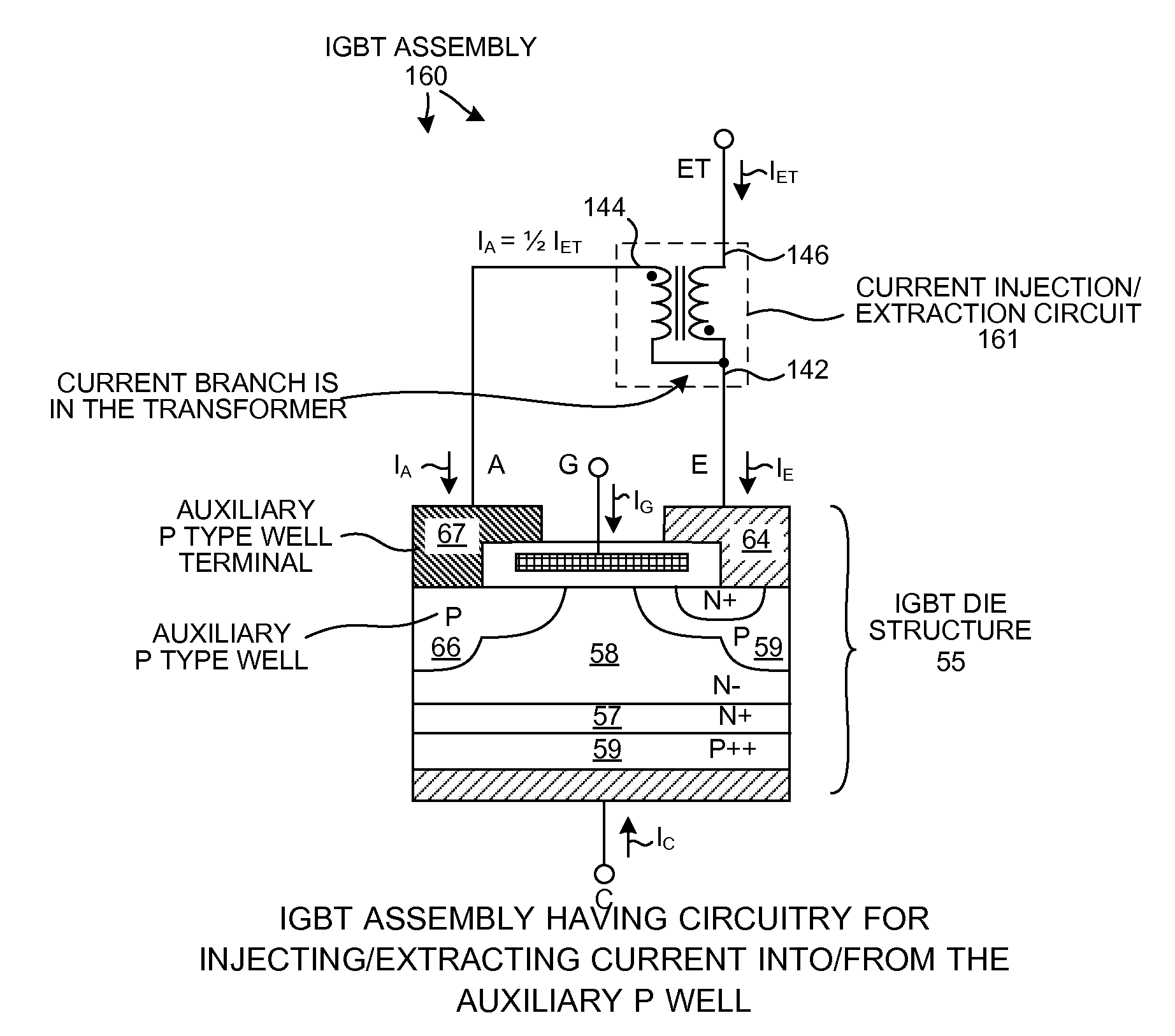
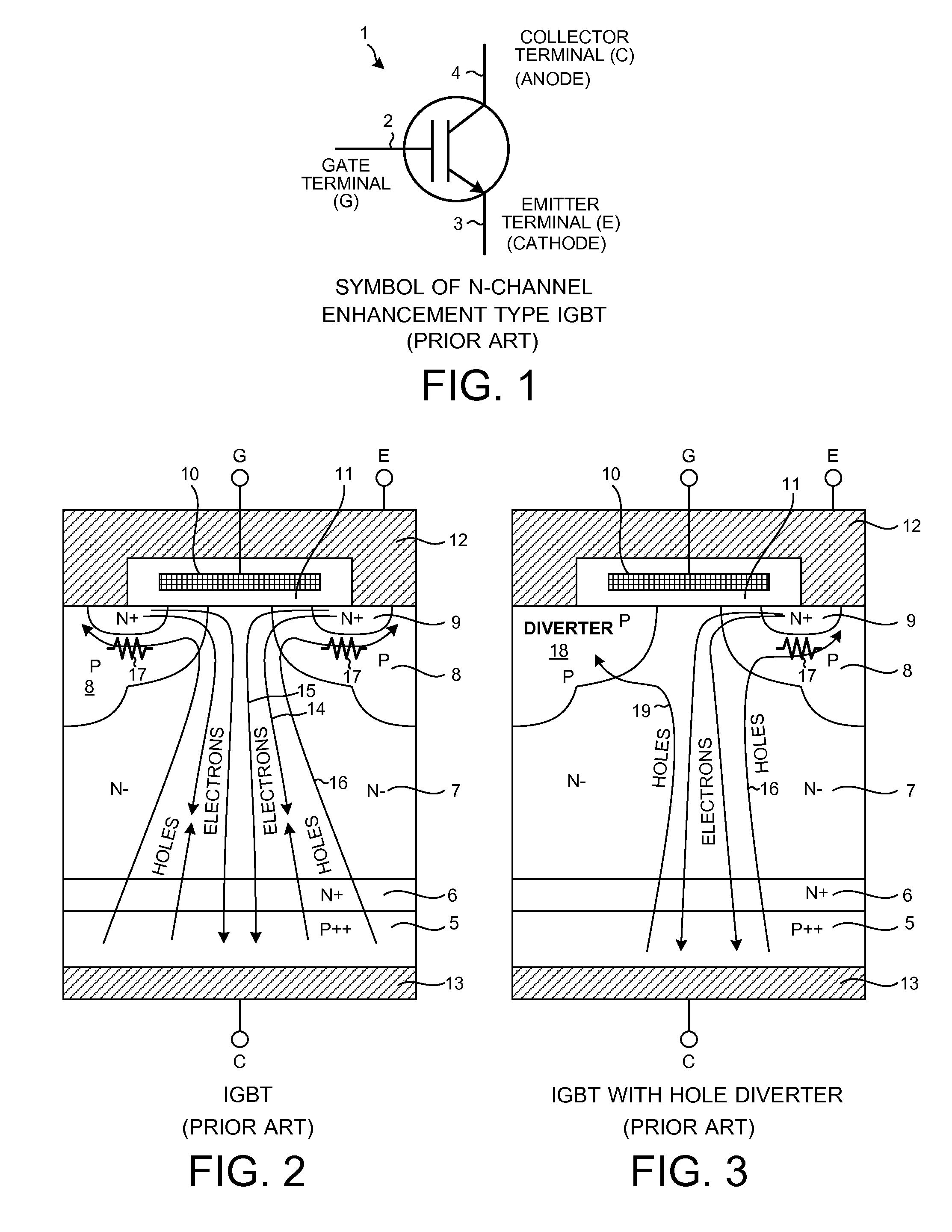
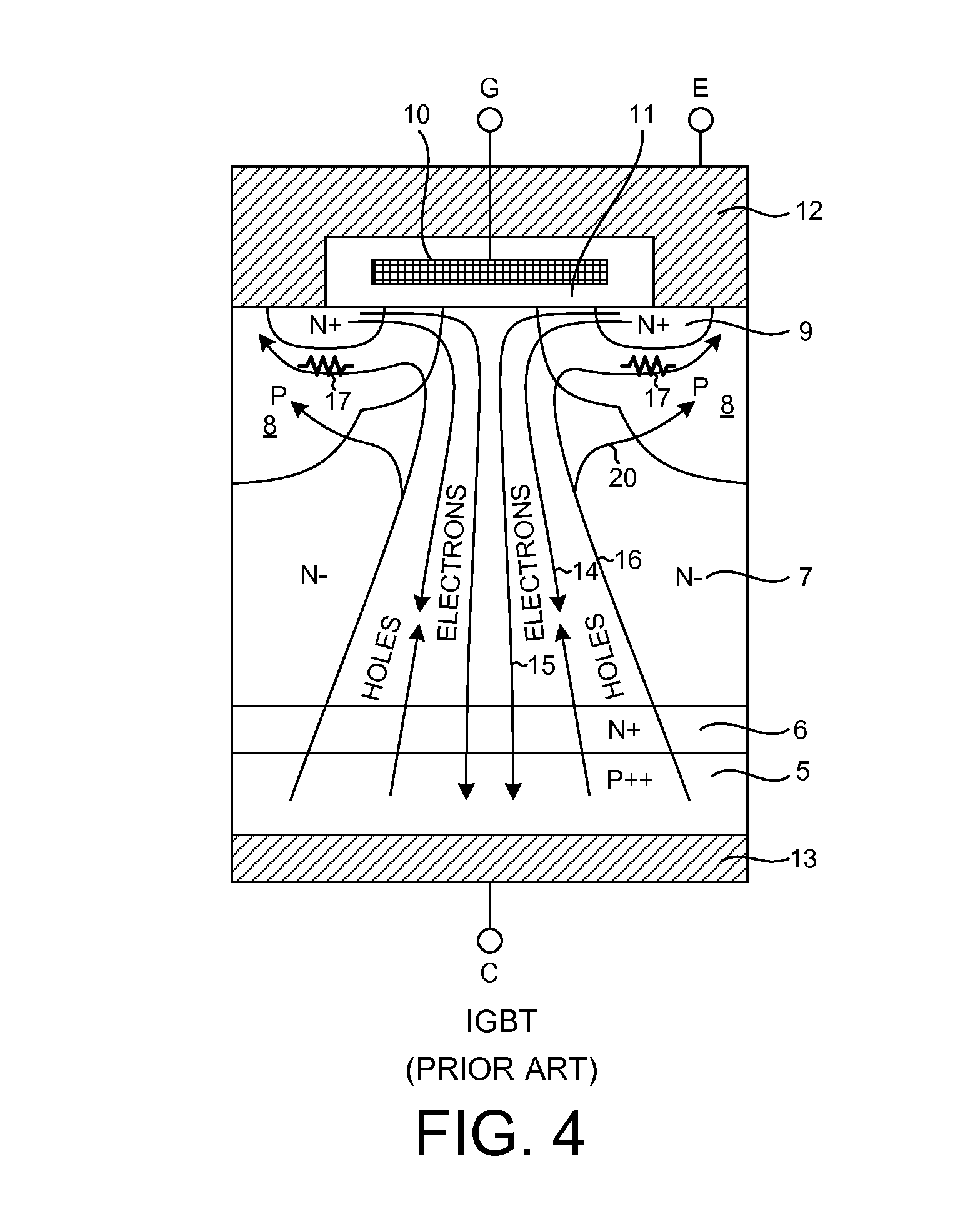
[0049]Reference will now be made in detail to background examples and some embodiments of the invention, examples of which are illustrated in the accompanying drawings. In the description and claims below, when a first object is referred to as being disposed “over” or “on” a second object, it is to be understood that the first object can be directly on the second object, or an intervening object may be present between the first and second objects. Similarly, terms such as “upper”, “top”, “up”, “down”, “bottom”, and “backside” are used herein to describe relative orientations between different parts of the structure being described, and it is to be understood that the overall structure being described can actually be oriented in any way in three-dimensional space. The notations N+, N−, N, P++, P+, and P are only relative, and are to be considered in context, and do not denote any particular dopant concentration range. A region denoted generally in the claims to be “P type”, however, ...


PUM


Abstract

An IGBT die structure includes an auxiliary P well region. A terminal, that is not connected to any other IGBT terminal, is coupled to the auxiliary P well region. To accelerate IGBT turn on, a current is injected into the terminal during the turn on time. The injected current causes charge carriers to be injected into the N drift layer of the IGBT, thereby reducing turn on time. To accelerate IGBT turn off, charge carriers are removed from the N drift layer by drawing current out of the terminal. To reduce VCE(SAT), current can also be injected into the terminal during IGBT on time. An IGBT assembly involves the IGBT die structure and an associated current injection / extraction circuit. As appropriate, the circuit injects or extracts current from the terminal depending on whether the IGBT is in a turn on time or is in a turn off time.

Description

TECHNICAL FIELD[0001]The described embodiments relate to Insulated Gate Bipolar Transistors (IGBTs).BACKGROUND INFORMATION[0002]FIG. 1 (Prior Art) is a symbol of an N-channel enhancement type Insulated Gate Bipolar Transistor (IGBT). There are several symbols in use for such an IGBT. FIG. 1 is but one of these symbols. Whereas in a power field effect transistor structure the current flow between drain and source is due primarily to the flow of majority carriers, in an IGBT structure the current flow between collector and emitter is due both to majority carrier flow and to minority carrier flow. Accordingly, for a given semiconductor die area, an IGBT can generally switch a larger current than a power field effect transistor of the same semiconductor die area. IGBTs are therefore preferable for certain applications. The IGBT symbol 1 includes a gate terminal 2, an emitter terminal 3, and a collector terminal 4.[0003]FIG. 2 (Prior Art) is a simplified cross-sectional diagram of an IGB...

Claims


Application Information

Patent Timeline
IPC IPC(8): H01L29/739H03K17/567H01L21/331
CPCH01L29/0834H01L2224/0603H01L2224/48091H01L2224/48247H01L2224/48472H01L2924/13055H01L2224/49096H01L23/495H01L24/06H01L24/48H01L24/49H01L2224/04042H01L2224/0616H01L2224/48105H01L2224/4813H01L2224/48177H01L2224/48265H01L2224/49111H01L2224/49175H01L2224/49176H01L2224/73265H01L2924/00014H01L2924/19104H01L2924/19107H01L29/41741H01L29/66333H01L29/0696H01L29/1095H01L29/4238H01L23/49562H01L2924/12036H01F38/30H01L2924/181H01L29/7395H01L2924/00012H01L2224/45099H01L2924/00
Inventor SEOK, KYOUNG WOOK
Owner LITTELFUSE INC
Why Eureka
Try Eureka