Organic light emitting diode display

Active Publication Date: 2014-03-20
SAMSUNG DISPLAY CO LTD
View PDF1 Cites 6 Cited by
  • Summary
  • Abstract
  • Description
  • Claims
  • Application Information

AI Technical Summary

Benefits of technology

This patent is about a new type of OLED display that is designed to protect against damage caused by external impact. The display has impact-absorbing lines and agents that are distributed throughout the surrounding layers. The impact absorption agent is concentrated towards the outer edge of the display, where it is most likely to be impacted. This helps to prevent damage to the display and ensures its durability.

Problems solved by technology

However, even if the impact absorption layer is installed, damage may still be easily generated at a sealant portion near the organic light emitting panel that is relatively weak against external impact.

Method used


Image

  • Organic light emitting diode display
  • Organic light emitting diode display
  • Organic light emitting diode display

Examples


Embodiment Construction

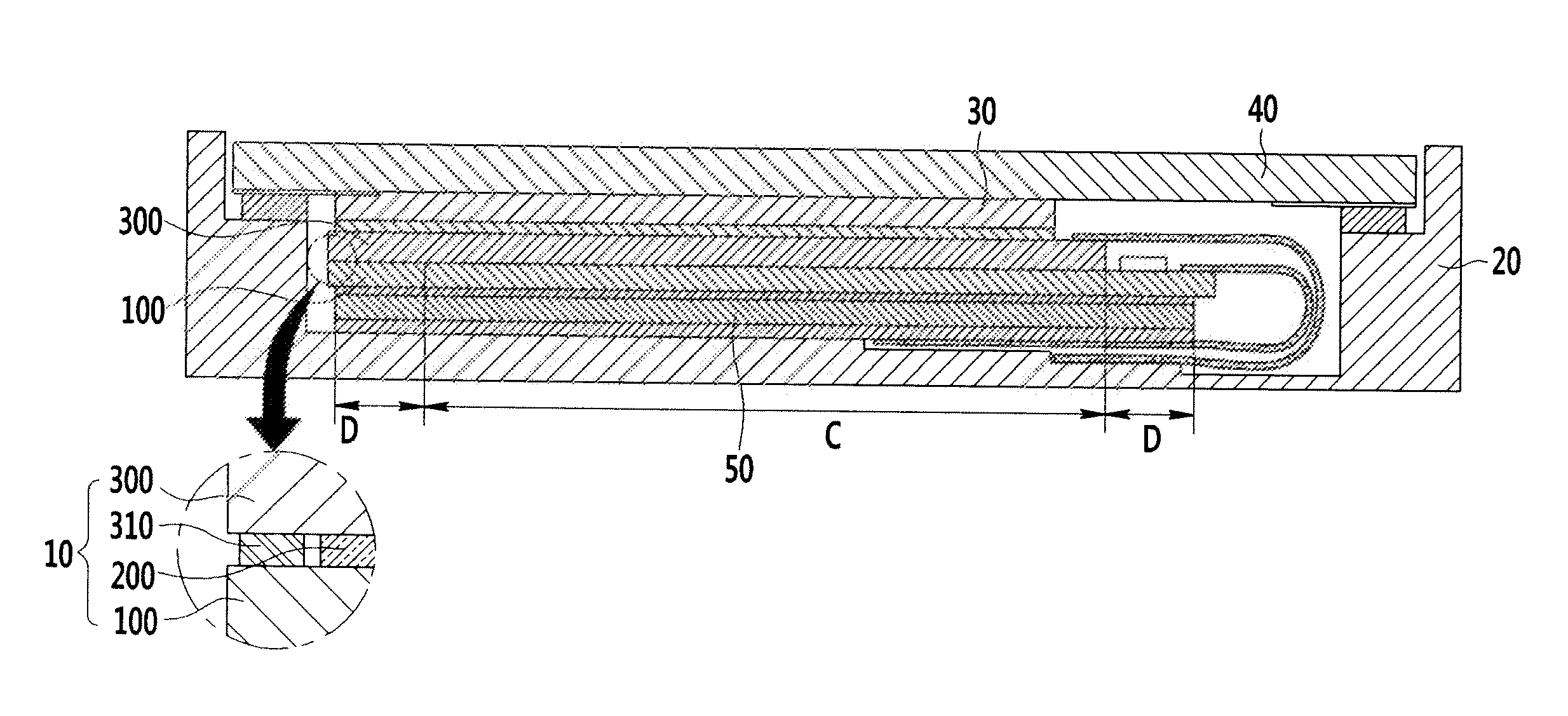
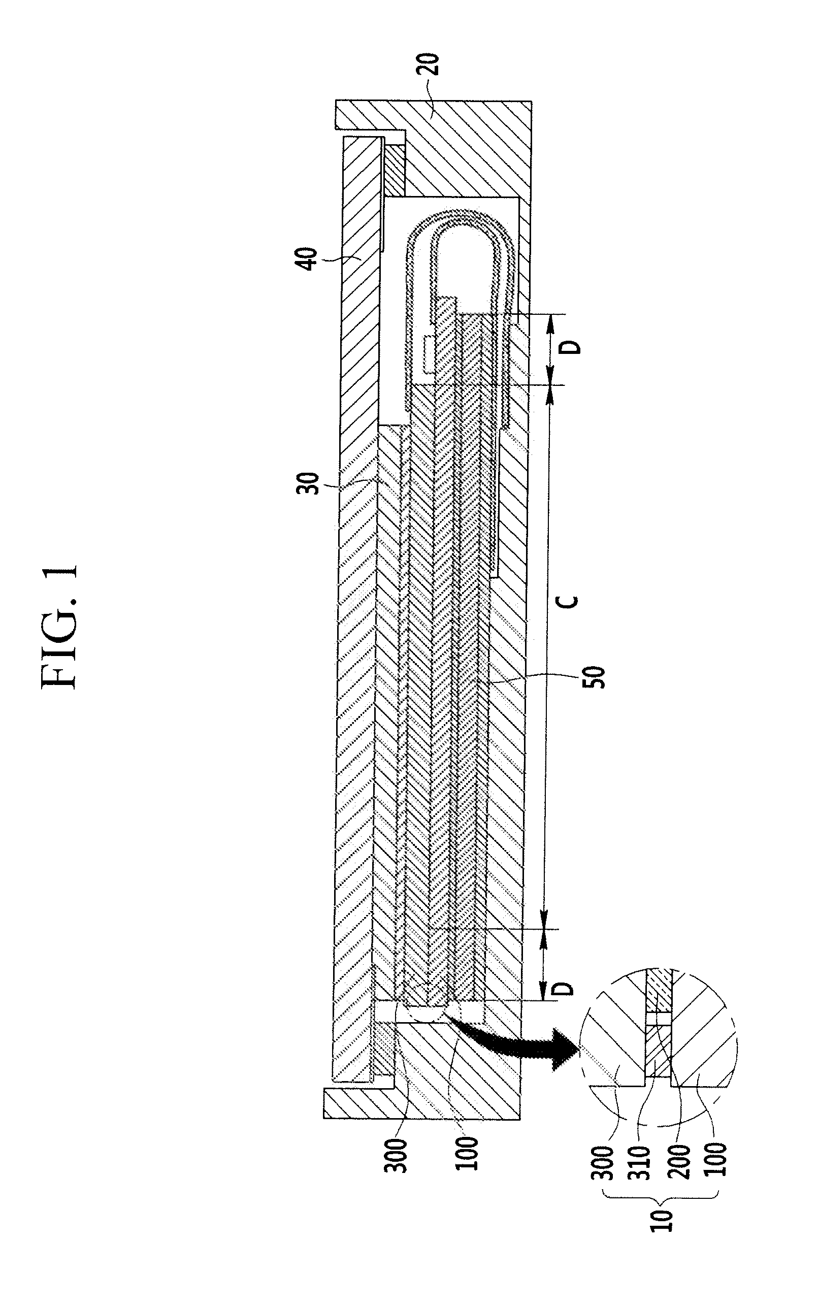
[0035]The present invention will be described more fully hereinafter with reference to the accompanying drawings, in which exemplary embodiments of the invention are shown. As those skilled in the art would realize, the described embodiments may be modified in various different ways, all without departing from the spirit or scope of the present invention.

[0036]The drawings and description are to be regarded as illustrative in nature and not restrictive. Like reference numerals designate like elements throughout the specification.

[0037]In order to clarify layers and regions, thicknesses and sizes thereof are exemplarily illustrated and thus the present invention is not limited thereto.

[0038]In the drawings, the thickness of layers, films, panels, regions, etc., are exaggerated for clarity. In addition, in order to clarify some layers and some regions, thicknesses and sizes thereof are enlarged in the drawings. It will be understood that when an element such as a layer, film, region, ...


PUM


Abstract

An organic light emitting diode (OLED) display according to an exemplary embodiment includes: a display substrate; an organic light emitting element on the substrate; a sealing member covering the organic light emitting element; a sealant formed between a surrounding portion of the display substrate and a surrounding portion of the sealing member; and an impact absorption layer under the display substrate, wherein an area ratio of the impact absorption agent in the impact absorption layer increases from the surrounding portion of the display substrate to a center of the display substrate such that the impact absorption ratio of the outer portion of the surrounding impact absorption layer is higher than the impact absorption ratio of the center impact absorption layer, and accordingly, damage to the surrounding portion of the display substrate that is weak against external impact may be prevented.

Description

CROSS-REFERENCE TO RELATED APPLICATION[0001]This application claims priority to and the benefit of Korean Patent Application No. 10-2012-0103952, filed in the Korean Intellectual Property Office on Sep. 19, 2012, the entire content of which is incorporated herein by reference.BACKGROUND[0002]1. Field[0003]The described technology relates generally to an organic light emitting diode (OLED) display.[0004]2. Description of the Related Art[0005]An organic light emitting diode (OLED) display includes an organic light emitting panel that includes an organic light emitting element. The organic light emitting element includes a plurality of OLEDs each formed of a hole injection electrode, an organic emission layer, and an electron injection electrode. Each OLED emits light by energy generated when excitons generated as electrons and holes are combined and dropped from an excited state to a ground state, and the OLED display displays an image by using the light.[0006]An organic light emittin...

Claims


Application Information

Patent Timeline
IPC IPC(8): H01L27/32
CPCH01L27/32Y02E10/549H10K77/10H10K59/87H10K59/131H10K59/8722H01L21/67369H01L33/52H10K39/32H10K59/00H10K50/84H10K50/841H10K59/12G02F1/133608
Inventor KIM, HWAN-JIN
Owner SAMSUNG DISPLAY CO LTD
Why Eureka
Try Eureka