Method for Making Porous Materials
a technology of porous materials and pore shapes, applied in the direction of liquid surface applicators, coatings, semiconductor devices, etc., can solve the problems of undesirable distortion of material structure, difficult control of pore shape and pore size, and only possible attainment of desired pore size and uniform distribution of pores, so as to reduce the dielectric constant. , the effect of reducing the dielectric constan
- Summary
- Abstract
- Description
- Claims
- Application Information
AI Technical Summary
Benefits of technology
Problems solved by technology
Method used
Image
Examples
example 2
Preparative Example 2
Porogen Modified by Surfactant
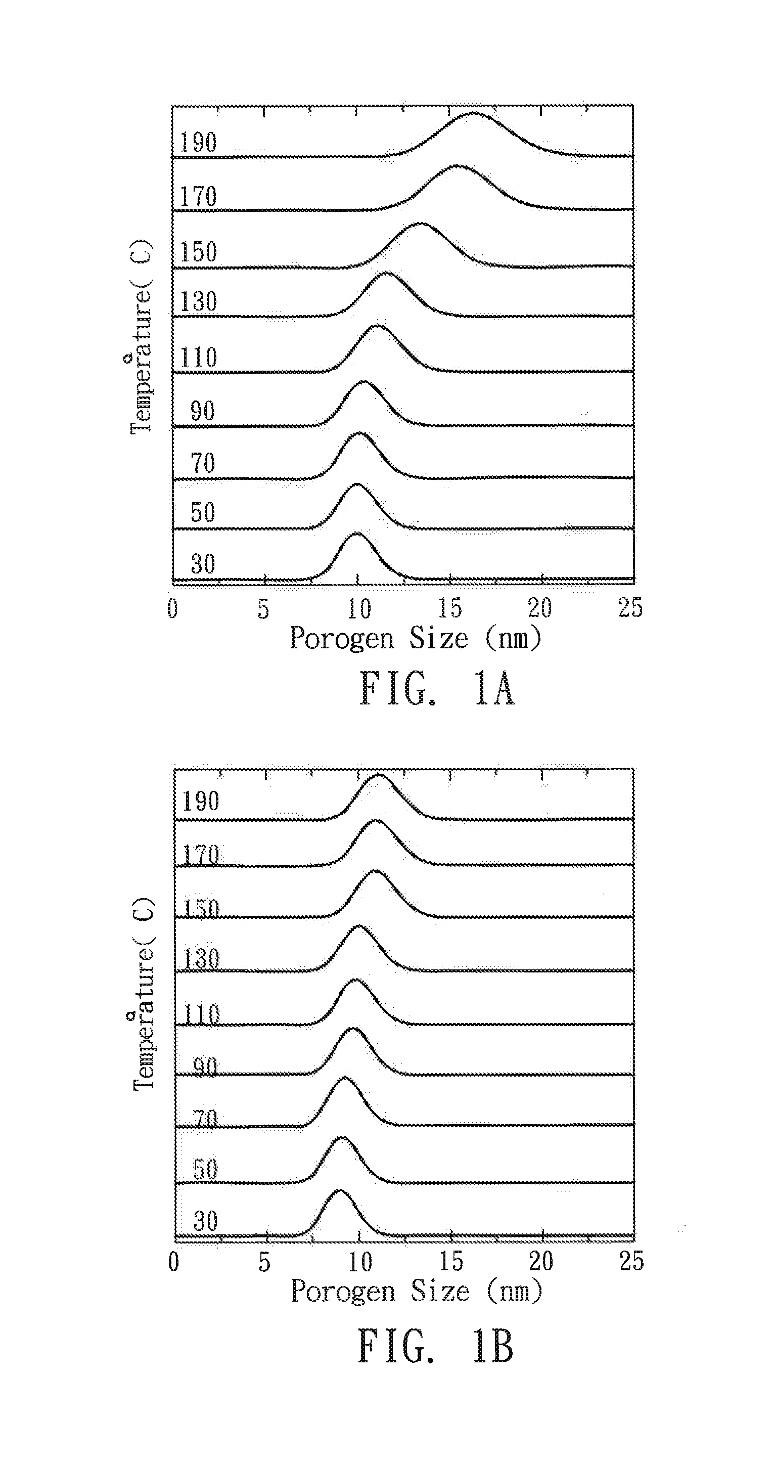
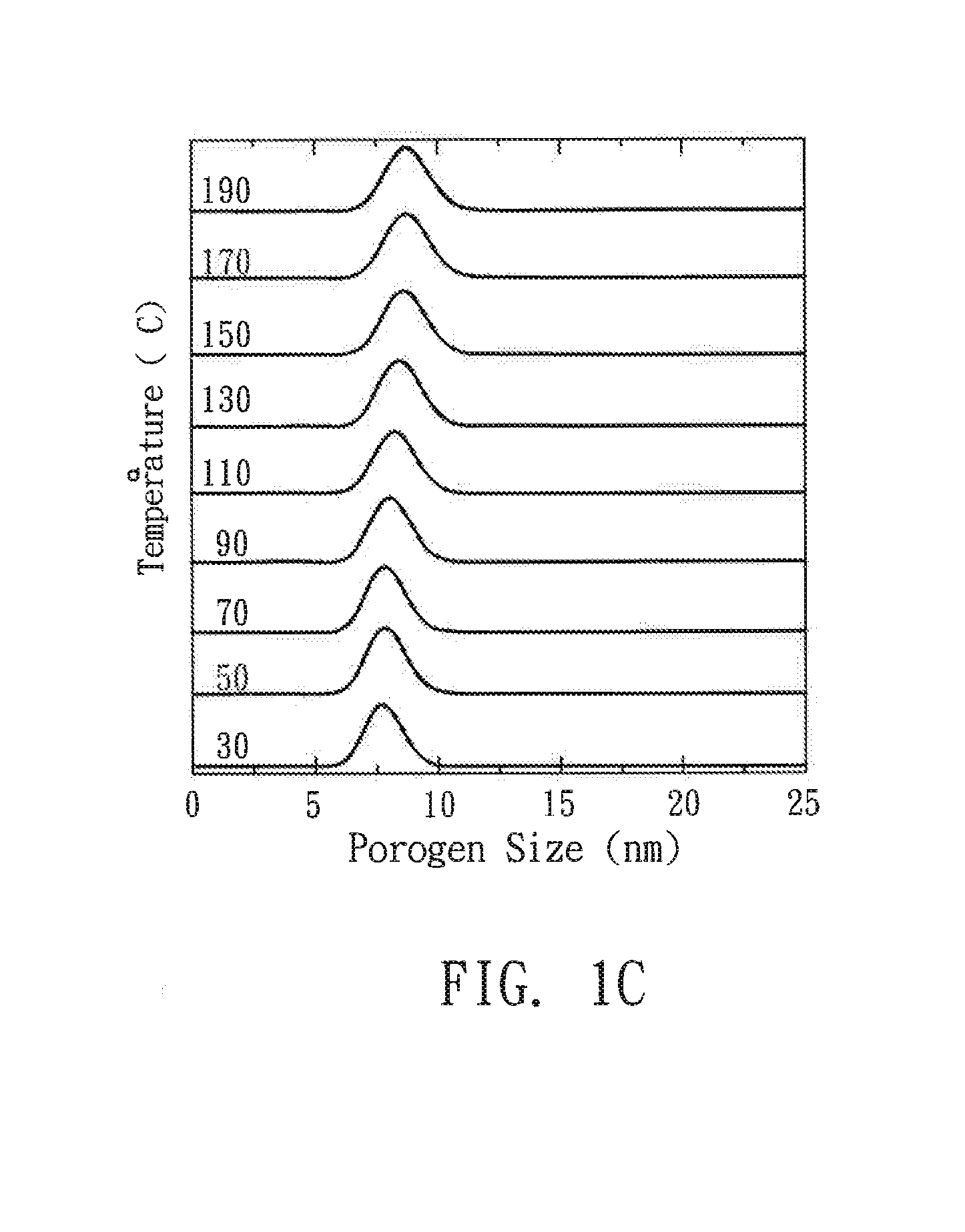
[0033]The PS / THF solution (of which pH being approximately 7) was prepared using the same method as in Preparative Example 1. Then, the PS particles were modified by anionic surfactant NaDBS (purchased from Showa Chemical Industrial Company, Mw=348.48, of which critical micelle concentration, CMC, being 522.75 mg / L) and cationic surfactant DB (purchased from Sigma-Aldrich, Mw=414.48 CMC=730.74 mg / L) below their CMC, respectively.
example 1
[0034]First, the zeta potentials of the PS particles prepared in Preparative Examples 1 and 2 were measured using a zeta potential analyzer (Zetasizer HSA 3000, purchased from Malvern Instruments), and the size of the PS particles in THF was measured using an ultrafine particle analyzer (Honeywell UPA 150).
[0035]Next, MSQ (purchased from Gelest) and PS particles (with and without surface modification) at 10 wt % loading were added to THF so as to form a low-k precursor solution. The low-k solution was filtered through a 0.20 gm PTFE filter (purchased from Millipore), and then spun onto a silicon wafer at 2000 rpm for 30 seconds under room temperature to obtain a 500 nm thick thin film. Lastly, the film was cured in a quartz tube furnace under N2 at a heating rate of 2° C. / min to 400° C. for 1 hour to form a porous material after completely burning out the porogens.
[Property Evaluation]
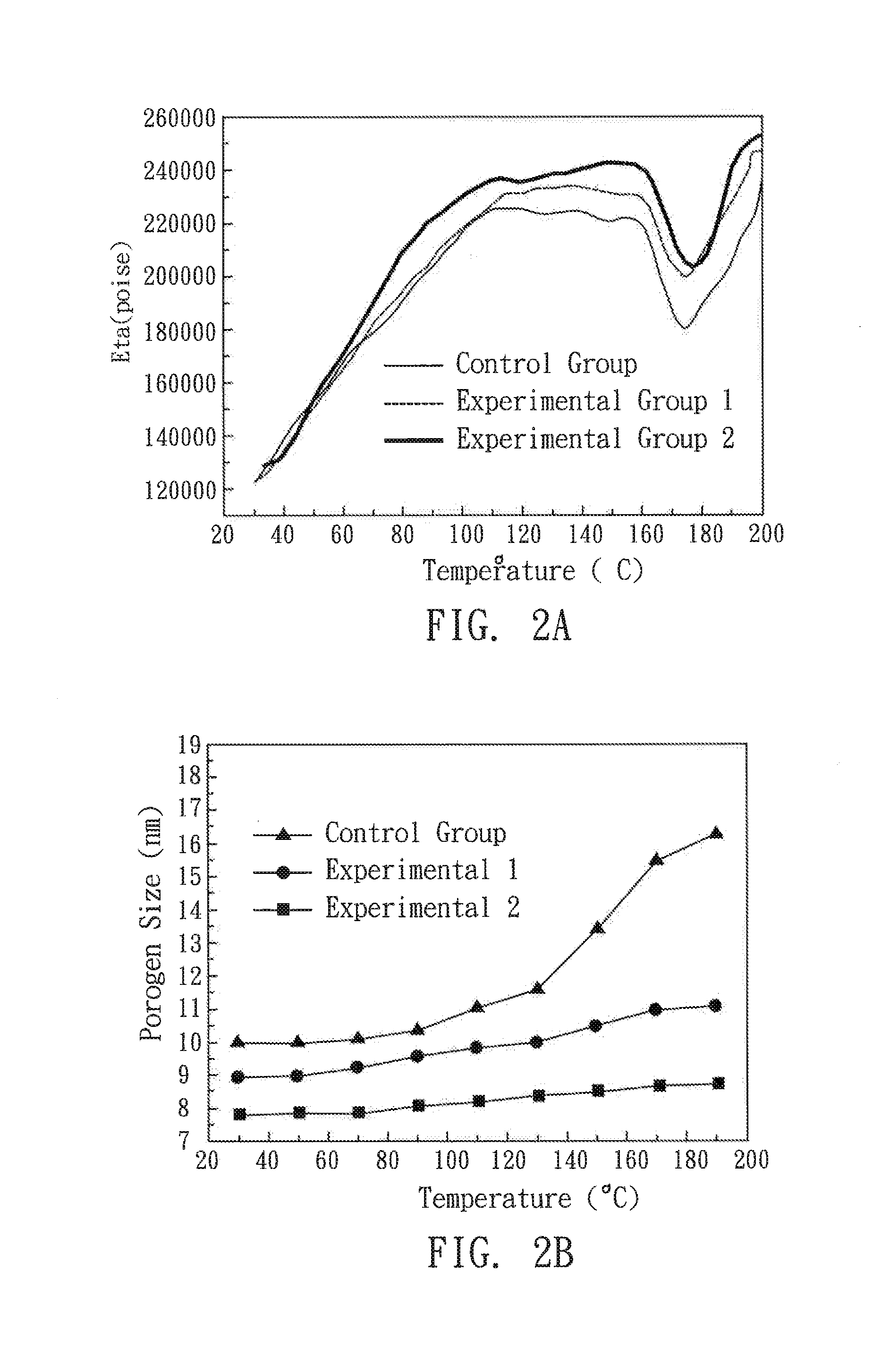
[0036]The size and distribution of the porogen in the film during the curing step were characterize...
PUM
| Property | Measurement | Unit |
|---|---|---|
| Temperature | aaaaa | aaaaa |
| Electric potential / voltage | aaaaa | aaaaa |
| Surface potential | aaaaa | aaaaa |
Abstract
Description
Claims
Application Information
 - R&D
- Intellectual Property
- Life Sciences
- Materials
- Tech Scout
- Unparalleled Data Quality
- Higher Quality Content
- 60% Fewer Hallucinations
Browse by: Latest US Patents, China's latest patents, Technical Efficacy Thesaurus, Application Domain, Technology Topic, Popular Technical Reports.
© 2025 PatSnap. All rights reserved.Legal|Privacy policy|Modern Slavery Act Transparency Statement|Sitemap|About US| Contact US: help@patsnap.com


