
Touch display panel

a display panel and touch technology, applied in the field of liquid crystal display technology, can solve the problems of conductive films, deformation of the performance of the two conductive films, limited viewing angle, etc., and achieve the effect of reducing the detection sensitivity of the touch display panel

Active Publication Date: 2014-01-23
SHANGHAI TIANMA MICRO ELECTRONICS CO LTD
View PDF4 Cites 17 Cited by
  • Summary
  • Abstract
  • Description
  • Claims
  • Application Information

AI Technical Summary

Benefits of technology

The invention provides a touch display panel that reduces interference between the driving lines and the upper electrode layer, as well as between the detecting lines and the upper electrode layer, which improves the sensitivity of detecting touch on the panel.

Problems solved by technology

However, according to the display principle of this display mode, the viewing angle is limited.
However, in the case where the resistive touch display panel is repeatedly pressed for a long time, the two conductive films may deform with the repeated pressing, and thereby the performance of the two conductive films may degrade or even the two conductive films may be damaged, which is prone to cause misjudgment of the touch signal.
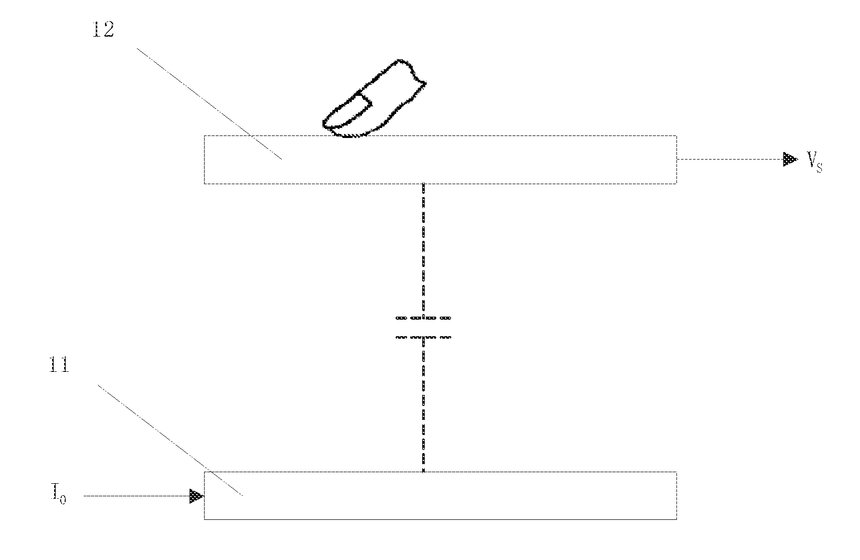
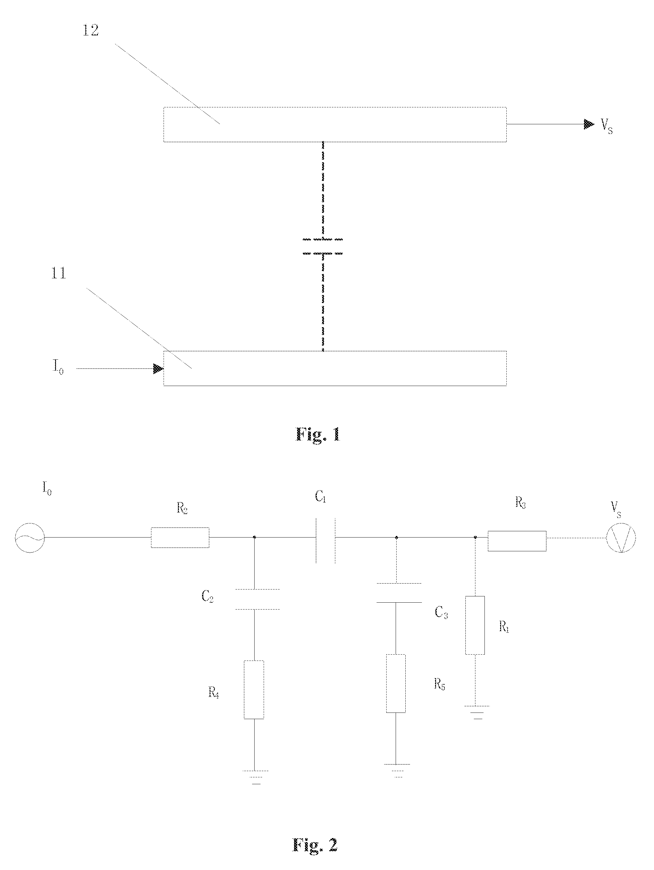
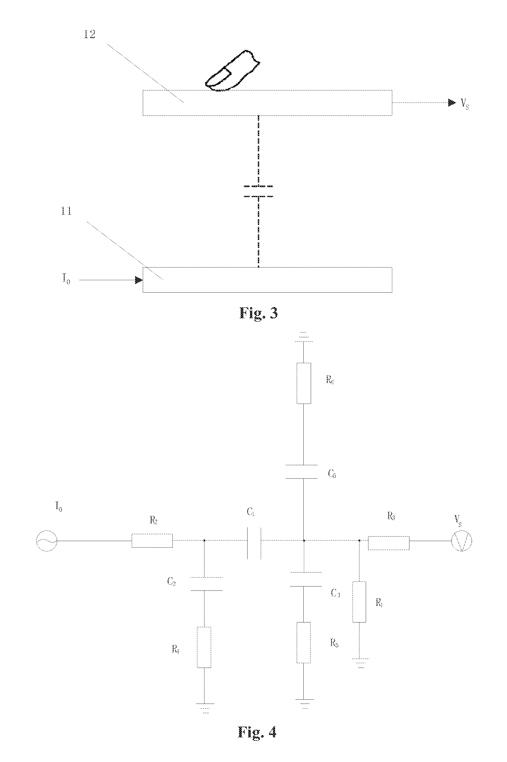
As for the above-mentioned touch detecting method, the parasitic capacitance may cause the voltage Vs detected from the detecting line to become smaller, therefore reducing the detection sensitivity of the touch display panel.
For the IPS-LCD touch display panel, the driving lines and the detecting lines disposed all over the entire layer may also lead to parasitic capacitances existed between the driving and detecting lines and the common and pixel electrodes which are separated, thus reducing the detection sensitivity of the touch display panel.

Method used


Image

  • Touch display panel
  • Touch display panel
  • Touch display panel

Examples


first embodiment

[0034]In the first embodiment, an IPS-LCD touch display panel which operates in the IPS liquid display mode is taken as an example to explain the technical solution of the invention.

[0035]Referring to FIG. 5, the IPS-LCD touch display panel includes: a color film (CF) substrate 2 and a thin film transistor (TFT) substrate 3 disposed opposite to each other, and a liquid crystal layer 4 disposed between the CF substrate and the TFT substrate.

[0036]The TFT substrate 3 is firstly described. Referring to FIG. 6 which is a plan view of a pixel unit and FIG. 7 which is a sectional view taken along line I-I in FIG. 6, the TFT substrate 3 includes a glass substrate 31 and a circuit board formed on the glass substrate 31. The surface of the circuit board close to the liquid crystal layer 4 is an electrode layer 32 including a common electrode 322 and a pixel electrode 321 which are used for providing a voltage to rotate the liquid crystal.

[0037]The circuit board includes a data line 34 and a ...

second embodiment

[0056]The structure of the touch display panel according to the second embodiment is substantially the same as the structure of the touch display panel according to the first embodiment, except that, for the CF substrate 2, the driving line 22 and detecting line 24 are disposed in one touch layer, rather than that the driving line 22 and the detecting line 24 are respectively disposed in two touch layers, as shown in FIG. 14. The driving line 22 and the detecting line 24 are isolated from each other via a dielectric layer 23. Furthermore, in the second embodiment, the driving line 22 separates the detecting line 24 into separate (individual) portions. On the separate portions, a first connecting portion (first bridging member) 25 is disposed to connect the separate portions of detecting line 24 across the driving line 22. In other embodiment, the detecting line 24 may also separate the driving line 22 into separate portions. A second connecting portion (second bridging member) is di...

third embodiment

[0061]The structure of the touch display panel according to the third embodiment is substantially the same as the structure of the touch display panel according to the first embodiment, the difference is that for the TFT substrate 3, the common electrode 322 and the gate line 33 are firstly formed on the glass substrate 31 and then the TFT structure and the pixel electrode 321 are formed. Therefore, the comb-shaped portion 3222 of the common electrode 322 and the comb-shaped portion 3212 of the pixel electrode 321 may not be formed in the same layer, as shown in FIG. 16, one or more insulating layer such as a passivation layer 37 is disposed between the comb-shaped portion 3222 of the common electrode 322 and the comb-shaped portion 3212 of the pixel electrode 321.

[0062]As for the case where the comb-shaped portion 3212 of the pixel electrode 321 is closer to the liquid crystal layer 4 than the comb-shaped portion 3222 of the common electrode 322 and the detecting line 24 is closer ...


PUM

PropertyMeasurementUnit
transparentaaaaaaaaaa
electrical controllabilityaaaaaaaaaa
electric fieldaaaaaaaaaa

Abstract

A touch display panel includes a color film (CF) substrate and a TFT substrate disposed opposite to each other, a liquid crystal layer disposed between the CF substrate and the TFT substrate. A common electrode having a comb-shaped structure and / or a pixel electrode having a comb-shaped structure are disposed on the TFT substrate close to the liquid crystal layer. The touch display panel further includes a touch layer disposed on the CF substrate close to the liquid crystal layer and having a driving line and a detecting line insulated from each other. The driving line and / or the detecting line have a comb-shaped structure that is at least partially misaligned with respect to the comb-shaped structure of the common electrode and / or the comb-shaped structure of the pixel electrode.

Description

CROSS-REFERENCES TO RELATED APPLICATIONS[0001]This application claims priority to and is a continuation of PCT / CN2012 / 085946, filed on Dec. 5, 2012 and entitled “TOUCH DISPLAY PANEL”, which claims the benefit of Chinese Patent Application No. 201210253996.8, filed with the Chinese Patent Office on Jul. 20, 2012 and entitled “TOUCH DISPLAY PANEL”, the contents of which are incorporated herein by reference in their entirety.FIELD OF THE INVENTION[0002]The present invention relates to the field of liquid crystal display technique, and in particular to a touch display panel.BACKGROUND OF THE INVENTION[0003]Liquid crystal has been increasingly applied in a display panel due to good electrical controllability of itself. For a liquid crystal display panel, among liquid crystal display modes, the twisted nematic (TN) display mode is most widely used. However, according to the display principle of this display mode, the viewing angle is limited. As a solution to this problem, it is known to ...

Claims


Application Information

Patent Timeline
Patent Type & Authority Applications(United States)
IPC IPC(8): G02F1/1333
CPCG02F1/13338G06F3/0412G06F3/0443G06F3/0446G06F3/0448G02F1/134318
Inventor WU, TIANYI
Owner SHANGHAI TIANMA MICRO ELECTRONICS CO LTD
Learn More