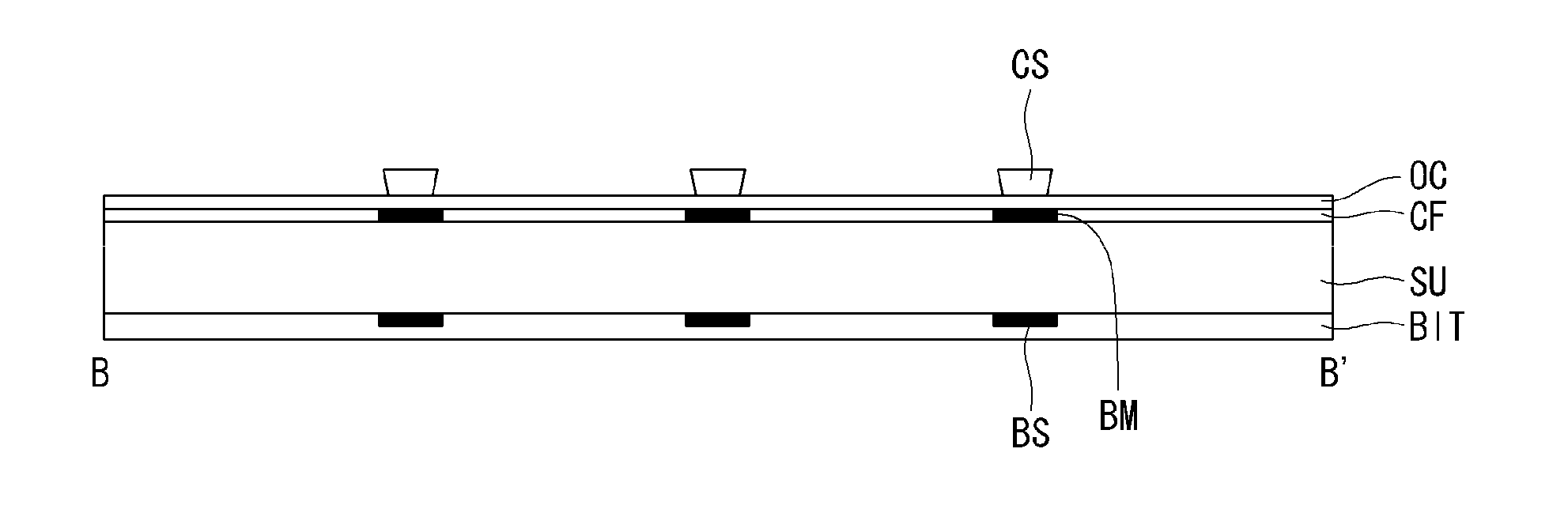
Patterned Retarder Type Display Device Having Black Strips and Manufacturing Method Therefor
- Summary
- Abstract
- Description
- Claims
- Application Information
AI Technical Summary
Benefits of technology
Problems solved by technology
Method used
Image

Examples
first embodiment
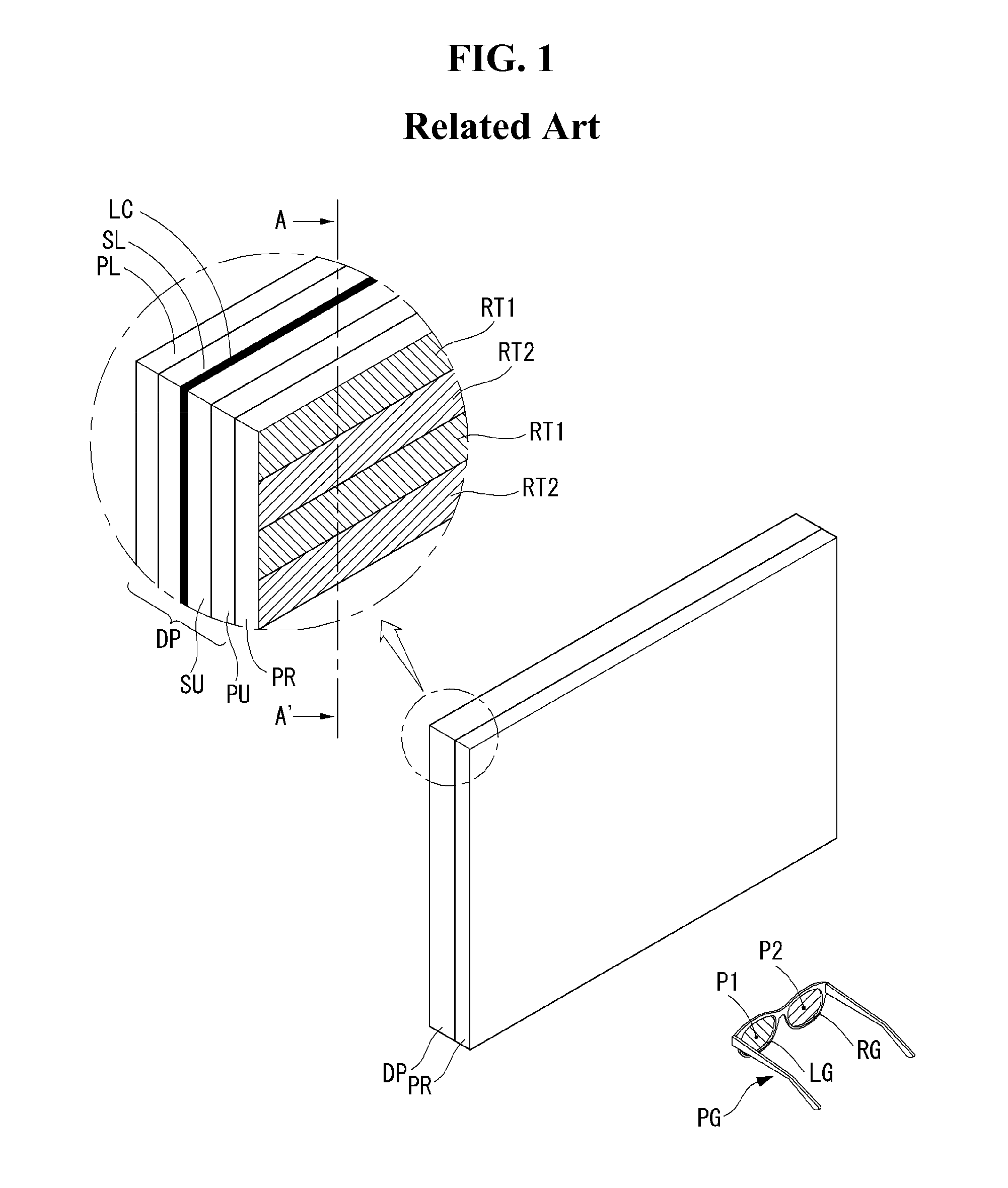
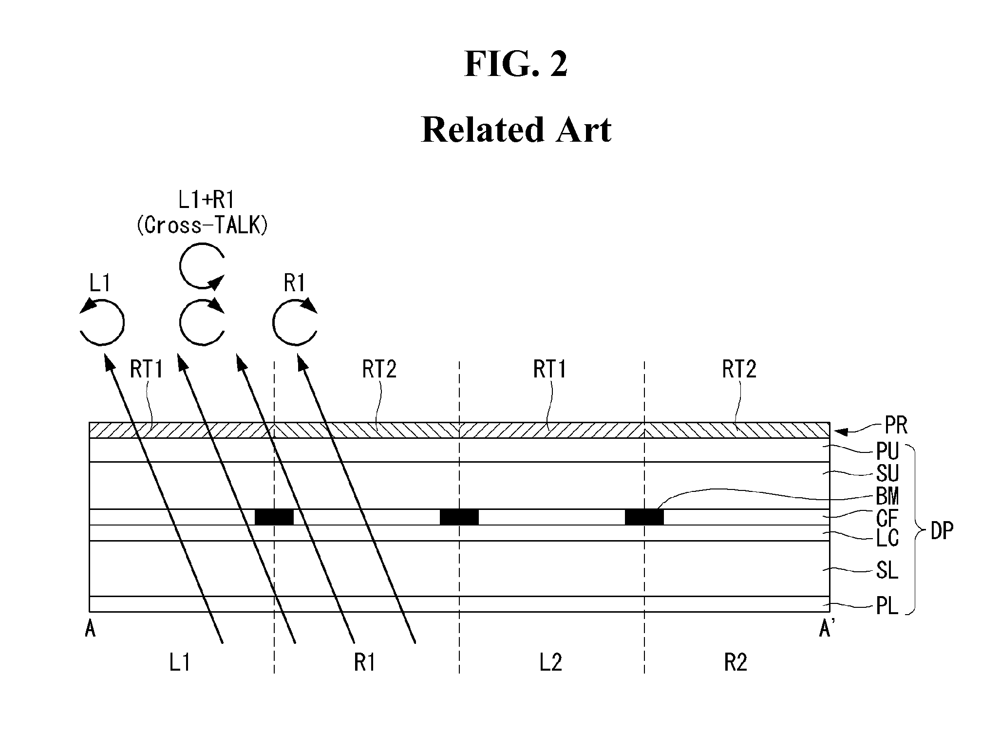
[0053]At first, referring to FIG. 4, the 3D display system according to the present disclosure represents the 3D images using the polarization characteristics of the patterned retarder PR disposed on the display panel DP and those of the polarization glasses PG used by the observer.
[0054]As shown in FIG. 4, the patterned retarder type 3D display system includes a display panel DP representing 2D image or 3D image, a patterned retarder PR attached on the front surface of the display panel DP, and polarization glasses PG. The display panel DP, as the device for displaying 2D video images and / or 3D video images, can include any one of the liquid crystal display device (or LCD), the field emission display (or FED), the plasma display panel (or PDP), the electroluminescence device (or EL) including the inorganic light emitting diode and the organic emitting diode (or OLED), and electrophoresis display device (or EPD). Hereinafter, we will explain the embodiments of the present disclosure...
second embodiment
[0076]Referring to FIGS. 7A to 7D, we will explain the method for manufacturing the patterned retarder type 3D display device having the black strips according to the present disclosure, in detail.
[0077]At first, for the thin film transistor substrate, a transparent lower substrate SL is prepared. As shown in FIG. 7A, on the inner surface of the transparent lower substrate SL, the pixel areas disposed in a matrix type are defined by forming the gate lines and the data lines crossing each other. In each pixel area, thin film transistor and the pixel electrode driven by the thin film transistor are formed. In the FIG. 7A, the layer including the display driving elements such as the thin film transistors and the pixel electrodes are illustrated as the thin film transistor layer TFL.
[0078]The thin film transistor layer TFL defining the pixel area is disposed in the display area AA for representing the video data. And, the outer area of the display area AA can be defined as the non-displ...
third embodiment
[0091]Referring to FIGS. 9A to 9D, we will explain the method for manufacturing the patterned retarder type 3D display device having the black strips according to the present disclosure, in detail.
[0092]At first, for the thin film transistor substrate, a transparent lower substrate SL is prepared. As shown in FIG. 9A, on the inner surface of the transparent lower substrate SL, the pixel areas disposed in a matrix type are defined by forming the gate lines and the data lines crossing each other. In each pixel area, thin film transistor and the pixel electrode driven by the thin film transistor are formed. In the FIG. 9A, the layer including the display driving elements such as the thin film transistors and the pixel electrodes are illustrated as the thin film transistor layer TFL, simply.
[0093]The thin film transistor layer TFL defining the pixel area is disposed in the display area AA for representing the video data. And, the outer area of the display area AA can be defined as the n...
PUM
 Abstract
Description
Claims
Application Information
 - R&D
- Intellectual Property
- Life Sciences
- Materials
- Tech Scout
- Unparalleled Data Quality
- Higher Quality Content
- 60% Fewer Hallucinations
Browse by: Latest US Patents, China's latest patents, Technical Efficacy Thesaurus, Application Domain, Technology Topic, Popular Technical Reports.
© 2025 PatSnap. All rights reserved.Legal|Privacy policy|Modern Slavery Act Transparency Statement|Sitemap|About US| Contact US: help@patsnap.com